In the highly specialized world of semiconductor manufacturing, every component plays a critical role in ensuring efficiency, precision, and yield. Among these, the 200mm wafer cassette stands out as a fundamental element in the production process. This article delves into the intricacies of the 200mm wafer cassette, exploring its significance, design, applications, and more. As the semiconductor industry continues to evolve with advancements in technology, understanding the role of the 200mm wafer cassette becomes paramount for professionals aiming to optimize their operations. Whether you're involved in fabrication, research, or supply chain management, this piece provides a comprehensive look at why the 200mm wafer cassette remains a staple in many facilities. We'll cover its history, key features, benefits, and future prospects, ensuring you gain a well-rounded perspective. By the end, you'll appreciate how this seemingly simple container contributes to the complex ecosystem of chip production. Let's dive into the details of the 200mm wafer cassette and its impact on the industry.
What Is a 200mm Wafer Cassette?
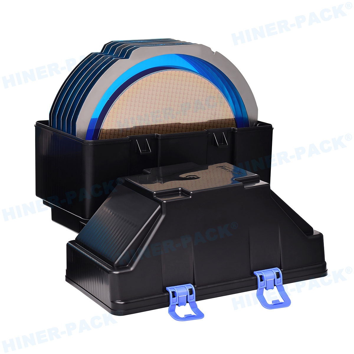
A 200mm wafer cassette is a specialized container designed to hold and transport silicon wafers that are 200 millimeters in diameter during various stages of semiconductor manufacturing. These cassettes, often made from high-purity materials like polycarbonate or stainless steel, provide a secure and clean environment for wafers, protecting them from contaminants, physical damage, and electrostatic discharge. The standard 200mm wafer cassette typically accommodates 25 wafers, though configurations can vary based on specific process requirements. In semiconductor fabs, the 200mm wafer cassette is integral to automated handling systems, enabling seamless movement between equipment such as etchers, deposition tools, and inspection stations. Its design includes precise slots to keep wafers separated and aligned, minimizing the risk of defects that could arise from contact or misalignment. As the industry has progressed, the 200mm wafer cassette has become synonymous with reliability, especially in legacy and mature process nodes where 200mm wafers are still widely used. Understanding the basics of the 200mm wafer cassette is the first step toward appreciating its broader role in manufacturing efficiency and product quality.
Historical Evolution of the 200mm Wafer Cassette
The history of the 200mm wafer cassette is closely tied to the evolution of semiconductor technology. In the 1990s, the industry transitioned from 150mm to 200mm wafers, driven by the need for higher productivity and cost-effectiveness. This shift necessitated the development of compatible handling solutions, leading to the standardization of the 200mm wafer cassette. Initially, cassettes were simple plastic carriers, but as processes became more complex, materials and designs evolved to meet stricter cleanliness and durability standards. The advent of automation in fab environments further refined the 200mm wafer cassette, incorporating features like RFID tags for tracking and anti-static properties to prevent charge buildup. Over the years, the 200mm wafer cassette has seen incremental improvements to support older fabrication lines that continue to operate efficiently, even as larger 300mm wafers gain prominence. This historical context highlights the resilience of the 200mm wafer cassette, which remains relevant due to its adaptability and the sustained demand for chips produced on 200mm lines, such as those for automotive and IoT devices. By tracing its development, we see how the 200mm wafer cassette has become a cornerstone of semiconductor history, bridging past innovations with present-day applications.
Design and Materials of 200mm Wafer Cassettes
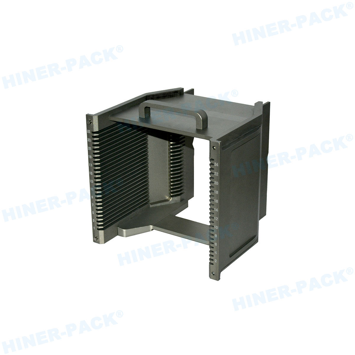
The design of a 200mm wafer cassette is meticulously engineered to ensure optimal performance in sensitive manufacturing environments. Typically, these cassettes feature a rectangular frame with evenly spaced slots that hold wafers in a vertical orientation, allowing for easy access by robotic arms. The materials used are critical; high-purity plastics like PEEK (polyether ether ketone) or conductive polymers are common to minimize particle generation and static electricity. For more demanding applications, metal-based 200mm wafer cassettes made from stainless steel or aluminum with protective coatings offer enhanced durability and heat resistance. Key design elements include smooth, rounded edges to prevent wafer chipping, as well as ventilation features to facilitate cleaning processes such as purging with inert gases. Additionally, modern 200mm wafer cassettes often incorporate smart features like barcodes or embedded sensors for real-time monitoring of wafer conditions. The precision in slot spacing—usually calibrated to sub-millimeter tolerances—ensures that wafers remain stable during high-speed transfers, reducing the risk of misalignment that could lead to yield loss. This attention to detail in the design and material selection of the 200mm wafer cassette underscores its importance in maintaining the integrity of semiconductor products throughout the production cycle.
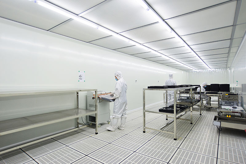
Applications in Semiconductor Manufacturing
In semiconductor manufacturing, the 200mm wafer cassette is ubiquitous across multiple process stages, from wafer fabrication to final testing. It serves as the primary carrier in front-end operations, such as lithography, where wafers are coated with photoresist and exposed to patterns. The 200mm wafer cassette ensures that wafers are delivered to steppers and scanners without contamination, which is crucial for achieving fine feature sizes. During etching and deposition processes, the cassette protects wafers from chemical exposure and mechanical stress, while in cleaning steps, it allows for efficient batch processing in wet benches. Back-end applications include assembly and packaging, where the 200mm wafer cassette facilitates the transfer of diced chips to bonding equipment. Moreover, in quality control and metrology, inspectors rely on the cassette to organize wafers for defect analysis and electrical testing. The versatility of the 200mm wafer cassette extends to research and development labs, where it supports prototyping and small-scale production runs. As the industry sees a resurgence in 200mm capacity for specialized chips—like power semiconductors and MEMS devices—the 200mm wafer cassette continues to be a workhorse, enabling cost-effective and flexible manufacturing solutions. Its broad applicability highlights why understanding the 200mm wafer cassette is essential for anyone involved in the semiconductor value chain.
Advantages of Using 200mm Wafer Cassettes
The advantages of using 200mm wafer cassettes are multifaceted, contributing to their enduring popularity in the semiconductor industry. Firstly, they offer exceptional cost efficiency, as the infrastructure for 200mm wafers is well-established and requires lower capital investment compared to newer, larger formats. This makes the 200mm wafer cassette ideal for fabs focusing on mature technologies or niche markets. Secondly, the compatibility of the 200mm wafer cassette with a wide range of existing equipment reduces the need for costly upgrades, allowing manufacturers to extend the lifecycle of their assets. Thirdly, the design promotes high throughput; by enabling batch handling of multiple wafers, the 200mm wafer cassette minimizes downtime and enhances overall productivity. Fourthly, its robust construction ensures reliability in harsh environments, reducing the frequency of replacements and maintenance. Lastly, the 200mm wafer cassette supports sustainability efforts by facilitating the reuse and recycling of materials, aligning with industry trends toward greener manufacturing. These benefits make the 200mm wafer cassette a strategic choice for companies aiming to balance innovation with operational practicality, ensuring that it remains a key component in the global semiconductor ecosystem.
Maintenance and Handling Best Practices
Proper maintenance and handling of 200mm wafer cassettes are vital to preserving wafer quality and extending the cassette's lifespan. Regular cleaning is essential to remove contaminants like particles, residues, or moisture that could compromise wafers. This often involves ultrasonic cleaning with deionized water or specialized solvents, followed by drying in a controlled environment to prevent static buildup. Handling should always occur in cleanrooms with appropriate ESD (electrostatic discharge) precautions, as static electricity can damage sensitive wafers. Operators must use trained techniques to load and unload wafers, avoiding physical contact that could cause scratches or breaks. Additionally, inspecting the 200mm wafer cassette for wear and tear—such as cracked slots or deformation—helps prevent mishaps during automation. Storage conditions also matter; cassettes should be kept in sealed containers when not in use to minimize exposure to airborne pollutants. Implementing a routine maintenance schedule for the 200mm wafer cassette, including periodic calibration and replacement of worn parts, ensures consistent performance and reduces the risk of production delays. By adhering to these best practices, manufacturers can maximize the efficiency and reliability of their 200mm wafer cassette investments, ultimately safeguarding their yield and product integrity.
Future Trends for 200mm Wafer Cassettes
Looking ahead, the future of 200mm wafer cassettes is shaped by ongoing industry dynamics and technological advancements. Despite the shift toward larger wafer sizes, the demand for 200mm wafers is expected to persist, particularly for applications in automotive, industrial, and IoT sectors, where legacy nodes are sufficient. This sustained demand will drive innovations in the 200mm wafer cassette, such as the integration of IoT connectivity for real-time tracking and predictive maintenance. Materials science may yield new composites that enhance cleanliness and durability, while designs could become more modular to support hybrid manufacturing setups. Additionally, as sustainability gains emphasis, recyclable and eco-friendly versions of the 200mm wafer cassette might emerge, reducing the environmental footprint of semiconductor operations. Collaborations between cassette manufacturers and fab operators will likely focus on customizing the 200mm wafer cassette for specific process needs, improving compatibility with advanced metrology tools. Overall, the 200mm wafer cassette is poised to evolve alongside the industry, adapting to new challenges and opportunities while maintaining its core role in efficient wafer management.
In summary, the 200mm wafer cassette is an indispensable component in semiconductor manufacturing, offering a blend of reliability, cost-effectiveness, and versatility. From its historical roots to its modern applications, the 200mm wafer cassette has proven essential for handling wafers with precision and care. As we've explored its design, advantages, and maintenance, it's clear that this tool will continue to play a significant role, especially in sectors reliant on 200mm technology. By staying informed about trends and best practices, professionals can leverage the 200mm wafer cassette to enhance their operations and drive innovation. Whether you're a veteran in the field or new to semiconductor processes, appreciating the value of the 200mm wafer cassette is key to navigating the complexities of chip production.
Frequently Asked Questions
Q1: What is the primary purpose of a 200mm wafer cassette?
A1: The primary purpose of a 200mm wafer cassette is to safely hold, transport, and store 200mm silicon wafers during semiconductor manufacturing processes. It protects wafers from contamination, physical damage, and electrostatic discharge, while facilitating efficient handling in automated systems.
Q2: How does a 200mm wafer cassette differ from cassettes for other wafer sizes?
A2: A 200mm wafer cassette is specifically designed for wafers that are 200 millimeters in diameter, with slot spacing and dimensions tailored to this size. In contrast, cassettes for larger wafers, like 300mm, are bigger and often include more advanced automation features, but the 200mm version is optimized for compatibility with older and specialized equipment.
Q3: What materials are commonly used in manufacturing 200mm wafer cassettes?
A3: Common materials for 200mm wafer cassettes include high-purity plastics such as polycarbonate and PEEK, as well as metals like stainless steel or aluminum. These materials are chosen for their cleanliness, durability, and ability to minimize static and particle generation in cleanroom environments.
Q4: Can 200mm wafer cassettes be reused, and how should they be maintained?
A4: Yes, 200mm wafer cassettes are often reusable. Proper maintenance involves regular cleaning with appropriate solvents or ultrasonic methods, inspection for damage, and storage in clean, sealed conditions. Following handling protocols and ESD precautions helps extend their lifespan and ensure consistent performance.
Q5: Why are 200mm wafer cassettes still relevant in today's semiconductor industry?
A5: 200mm wafer cassettes remain relevant due to the continued demand for chips produced on 200mm lines, especially in areas like power management, sensors, and analog devices. Their cost-effectiveness, compatibility with existing infrastructure, and reliability make them a practical choice for many manufacturers, even as larger wafer sizes gain traction.