
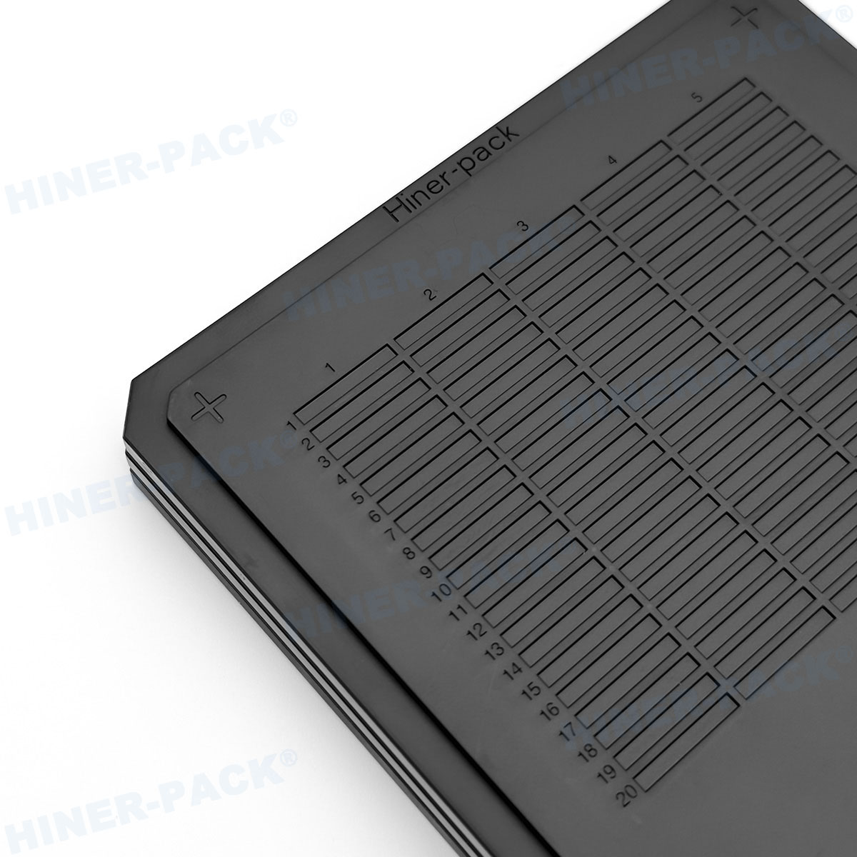
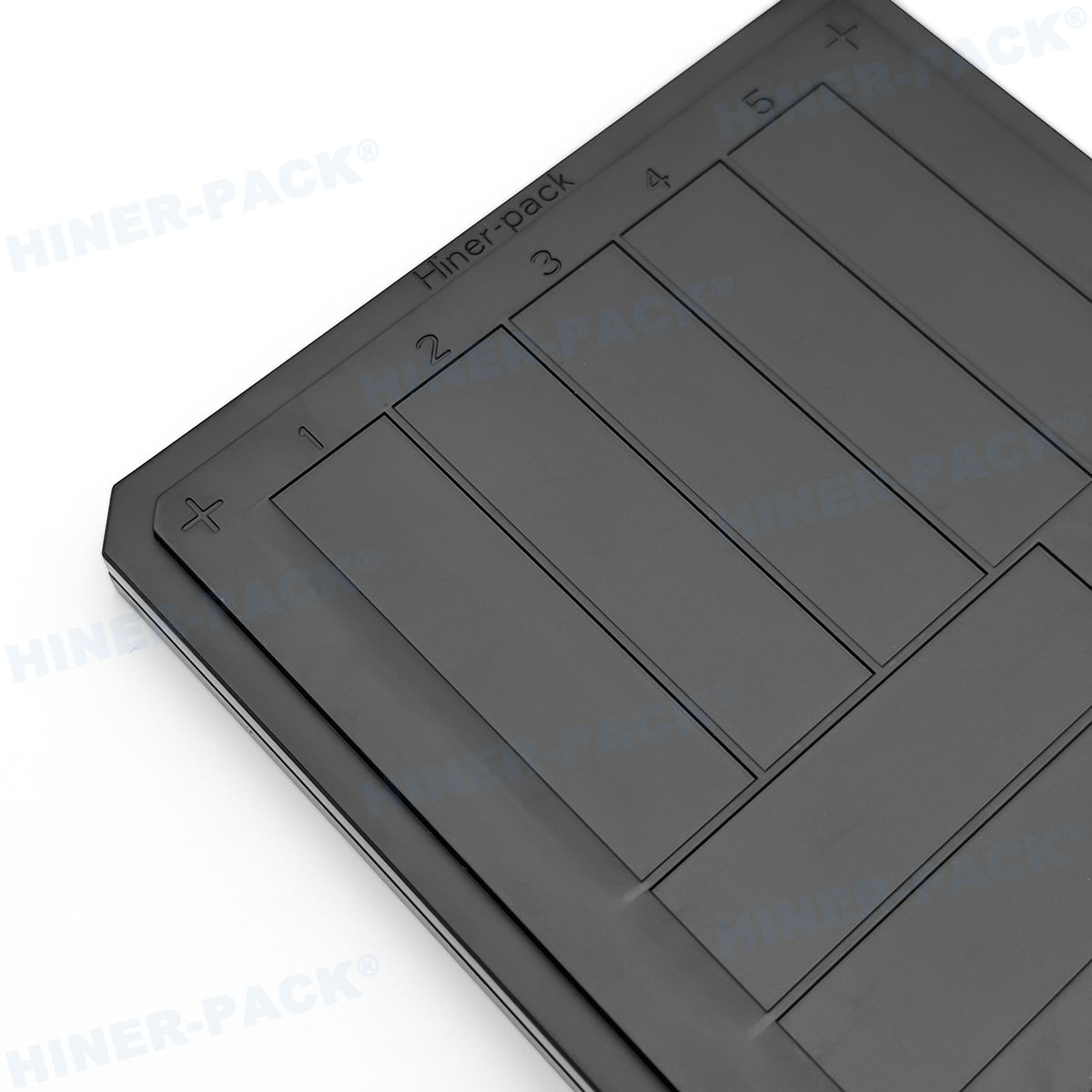
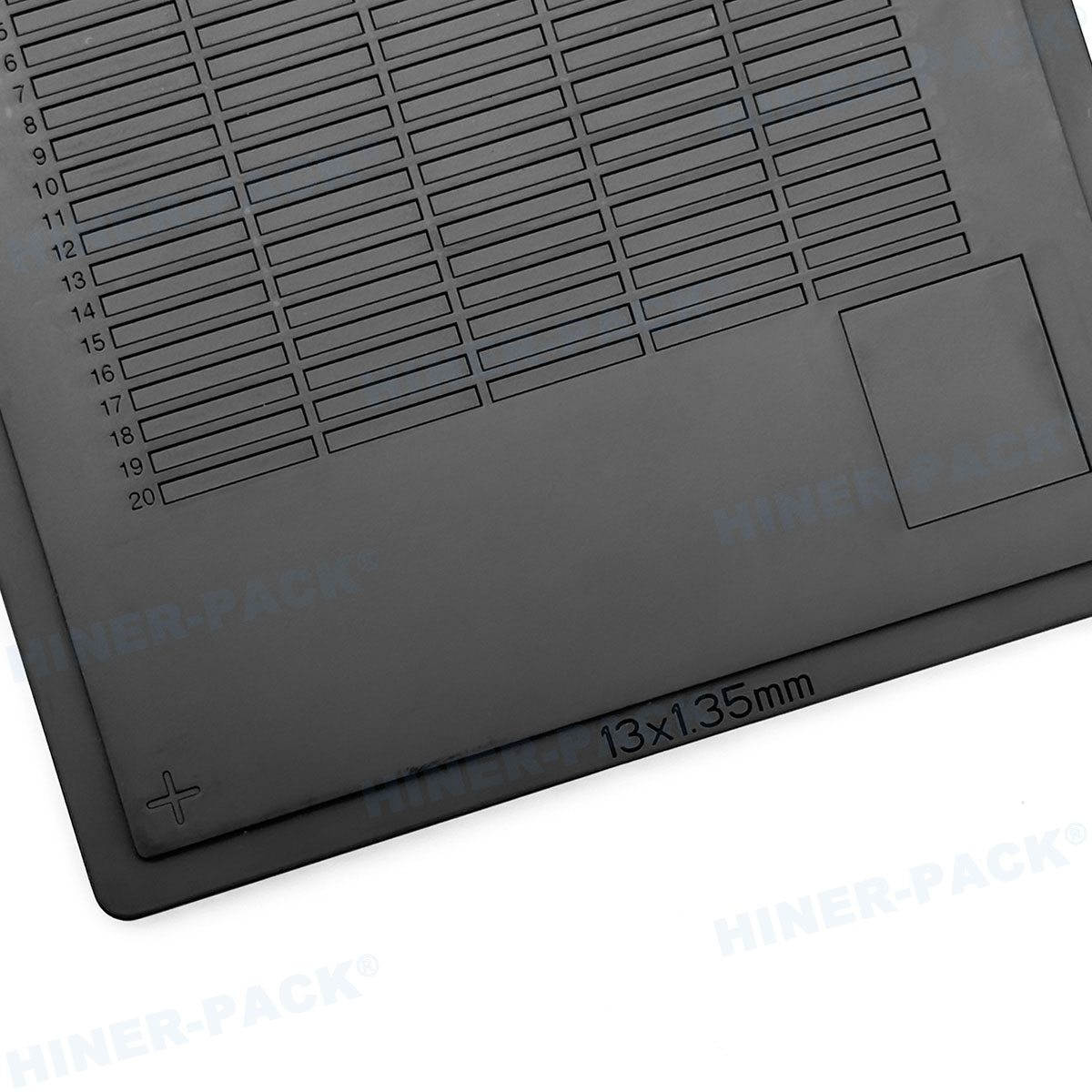
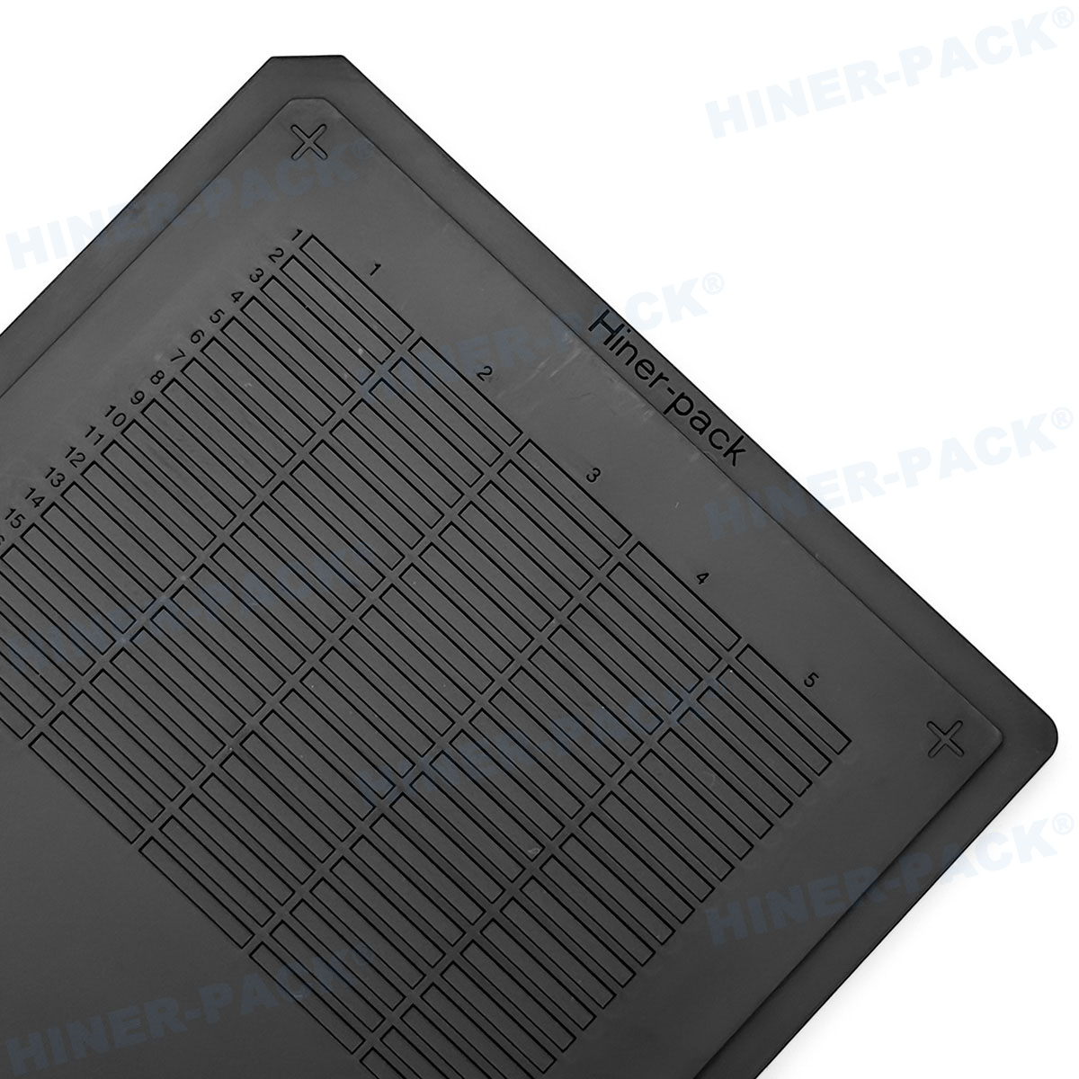
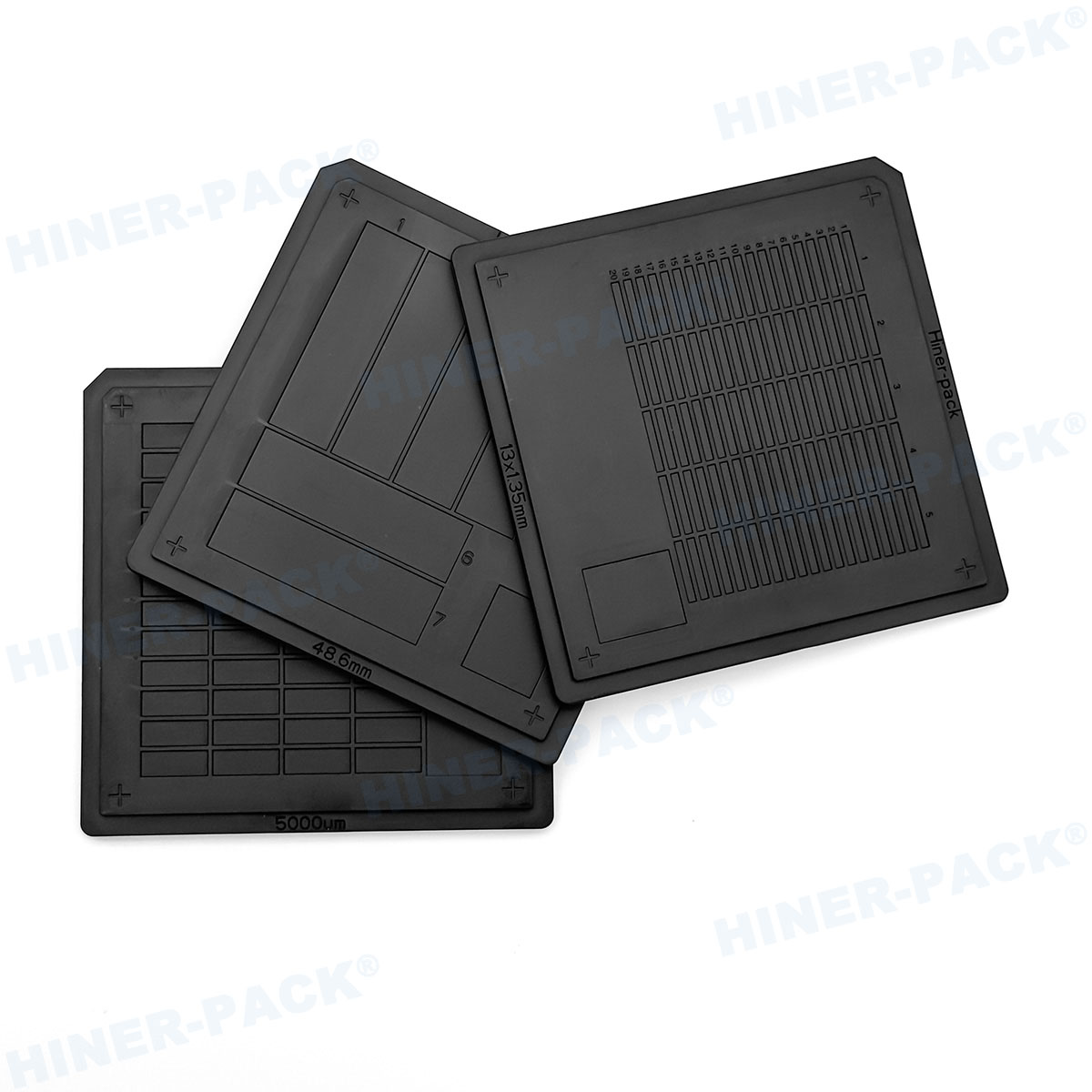
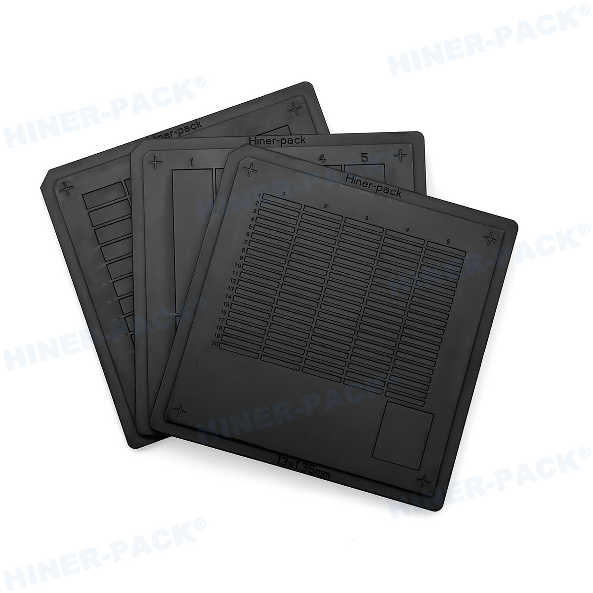
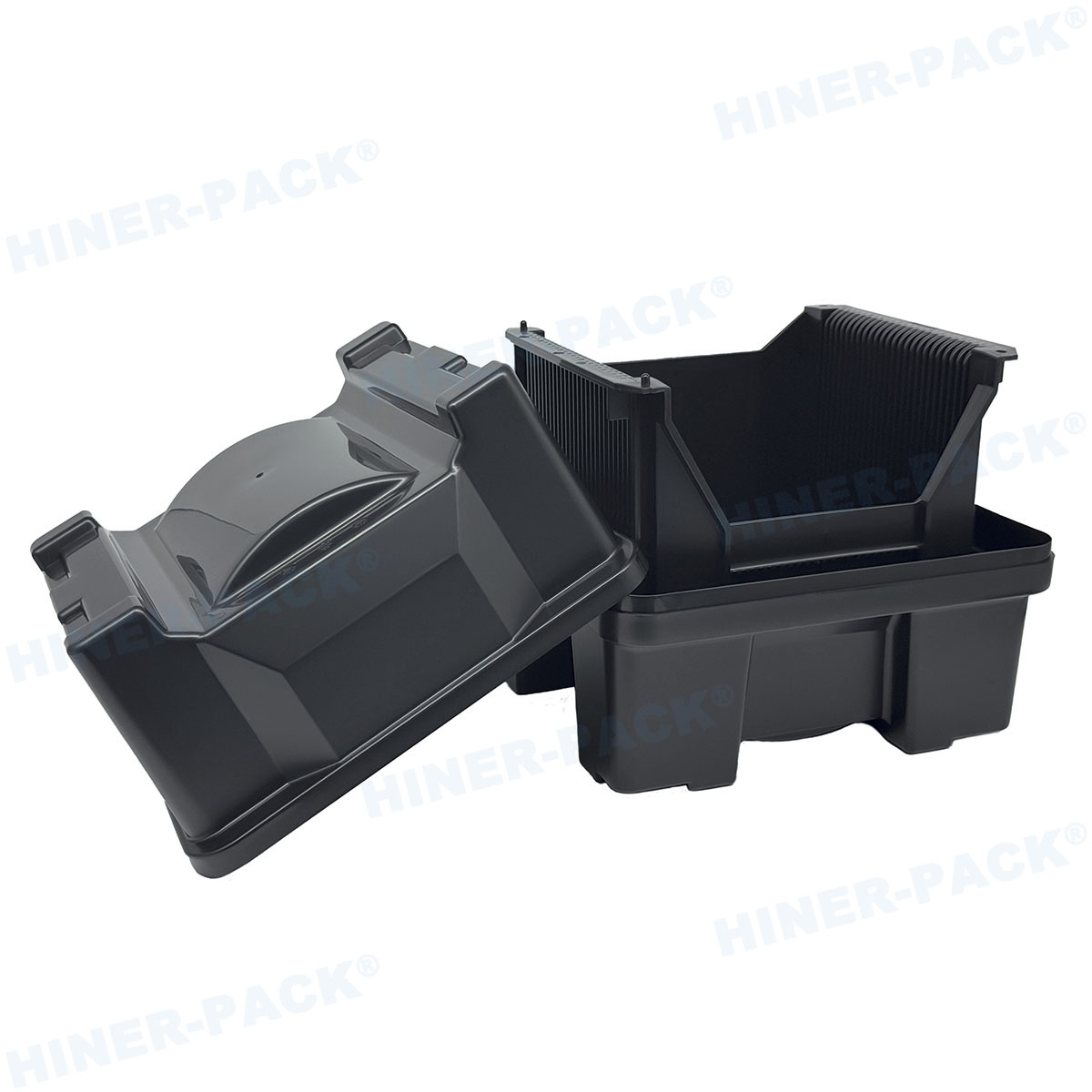
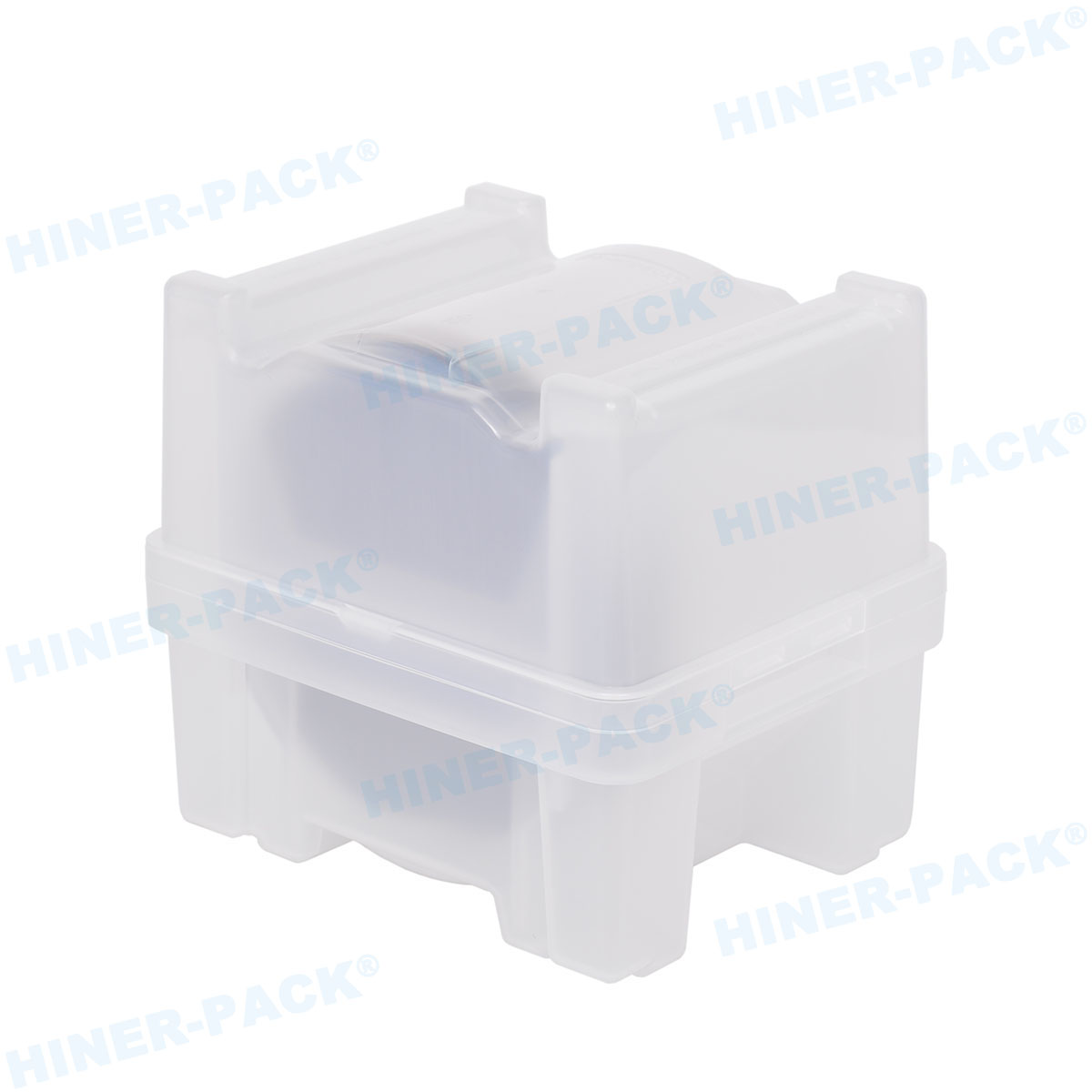
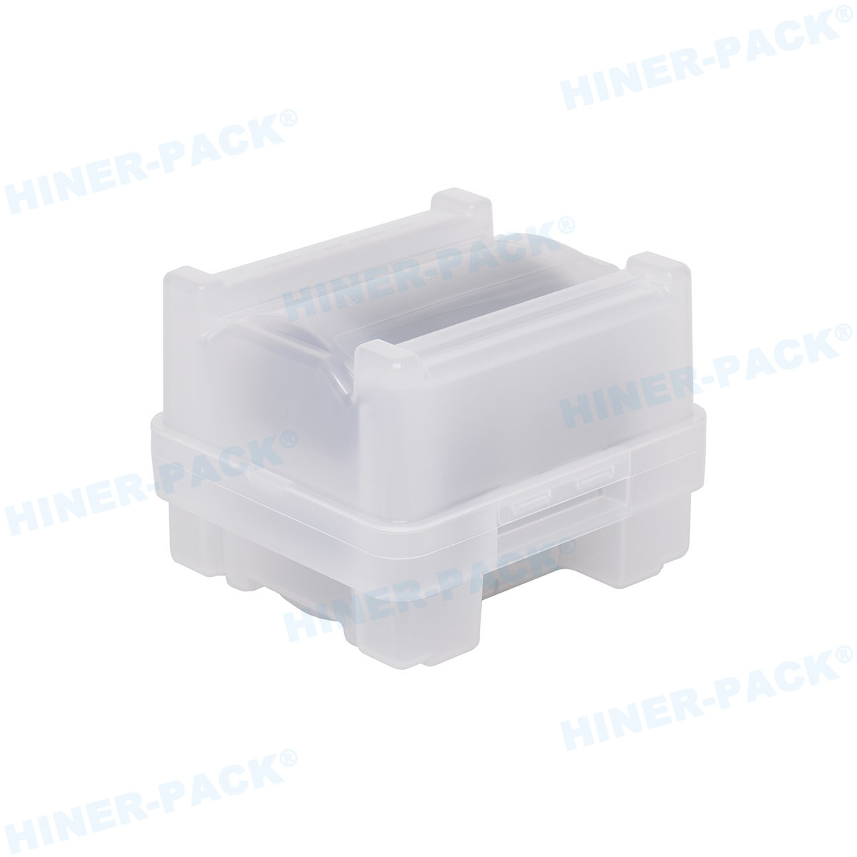
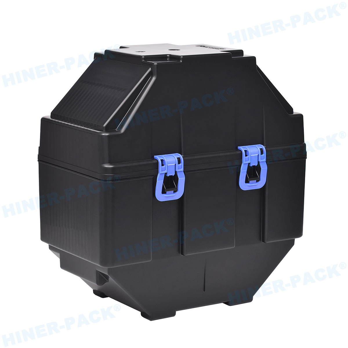
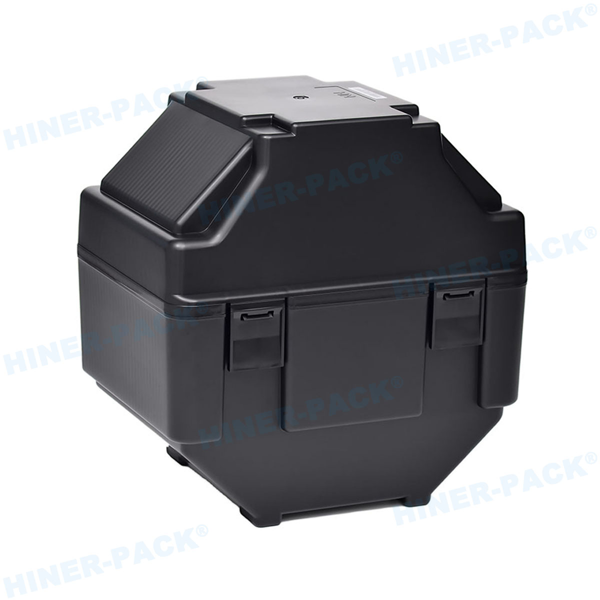
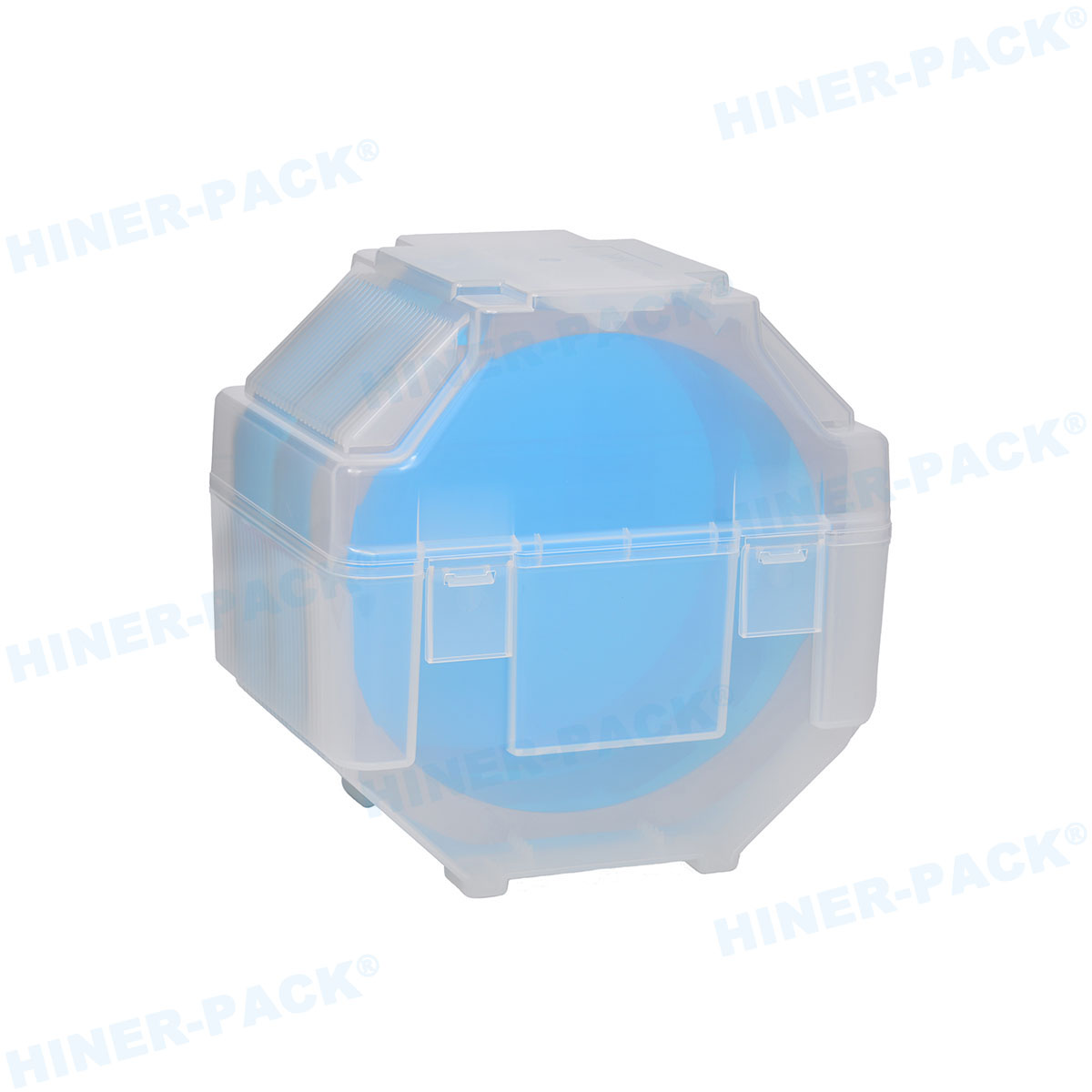
4-inch Bare Die Tray
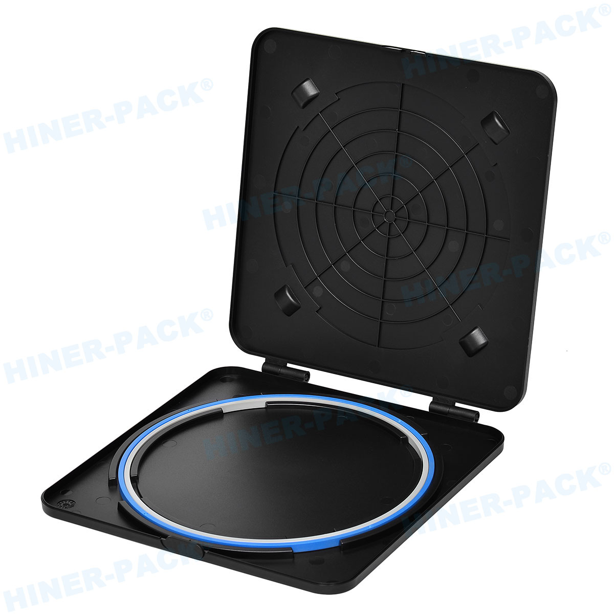
- Molded cavity grid prevents shift and micro-edge damage
- Static-dissipative or antistatic options curb ESD hazards
- Consistent depth and spacing aid robotic precision
- Low-particle, low-outgassing resin suits cleanroom protocols
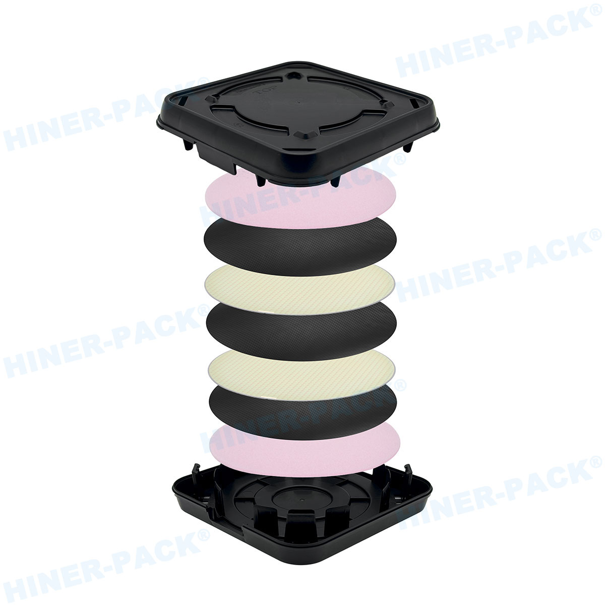
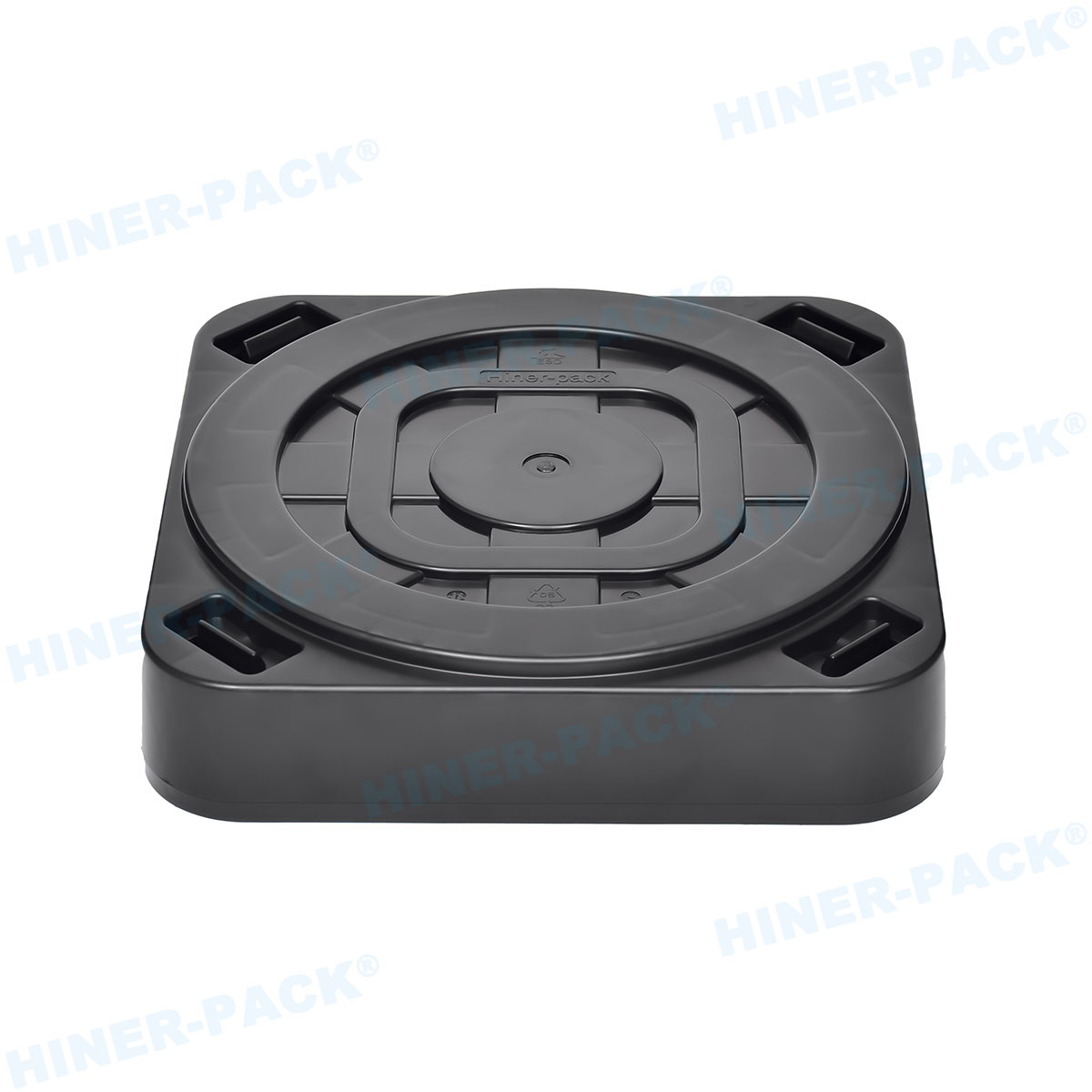
- Stackable, lightweight form saves space in storage and transport
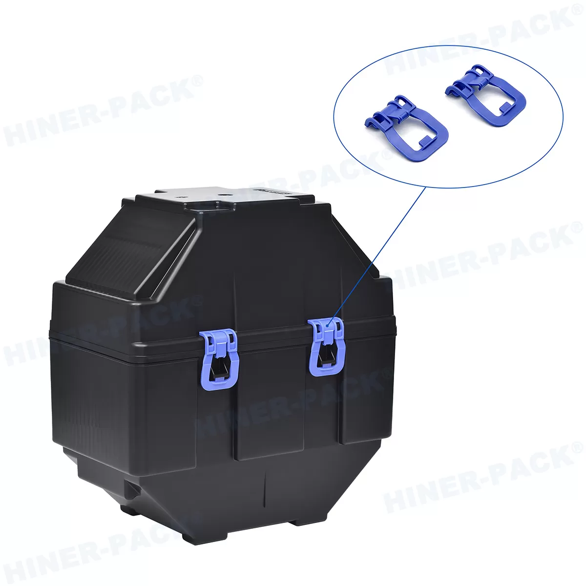
- Covers and clips available for transit security
- Static-dissipative or antistatic options curb ESD hazards
- Consistent depth and spacing aid robotic precision
- Low-particle, low-outgassing resin suits cleanroom protocols
- Stackable, lightweight form saves space in storage and transport
- Covers and clips available for transit security
×
Get a Quote
Please fill in all * fields below, we will get back to you as soon as possible.
 Video
Video
 Video
Video
 Video
Video
 Video
Video
 Video
Video
 Video
Video
 Video
Video
 Video
Video
 Video
Video
 Video
Video
 Video
Video
 Video
Video
 Video
Video
