- HOME
- ABOUT US
-
PRODUCTS
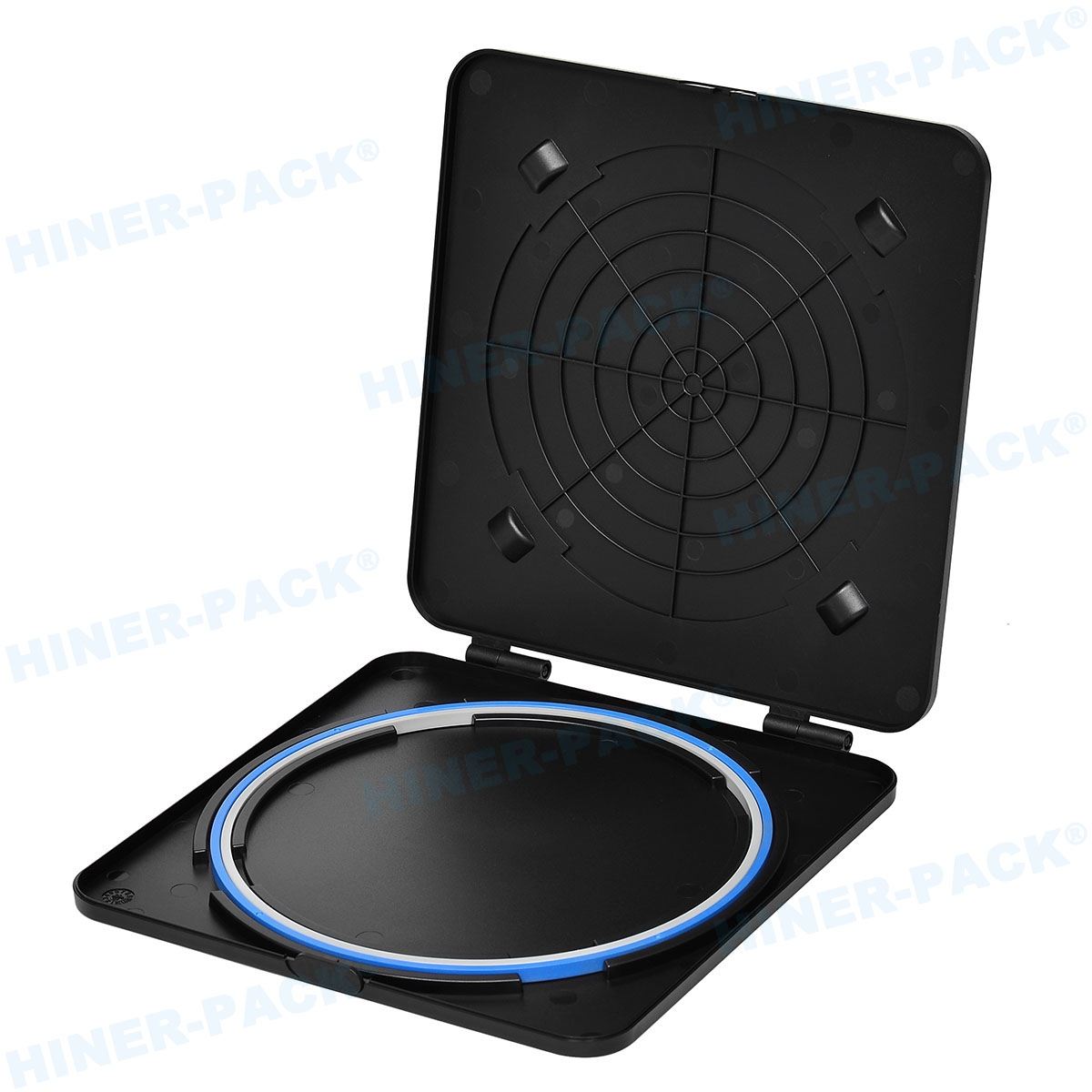
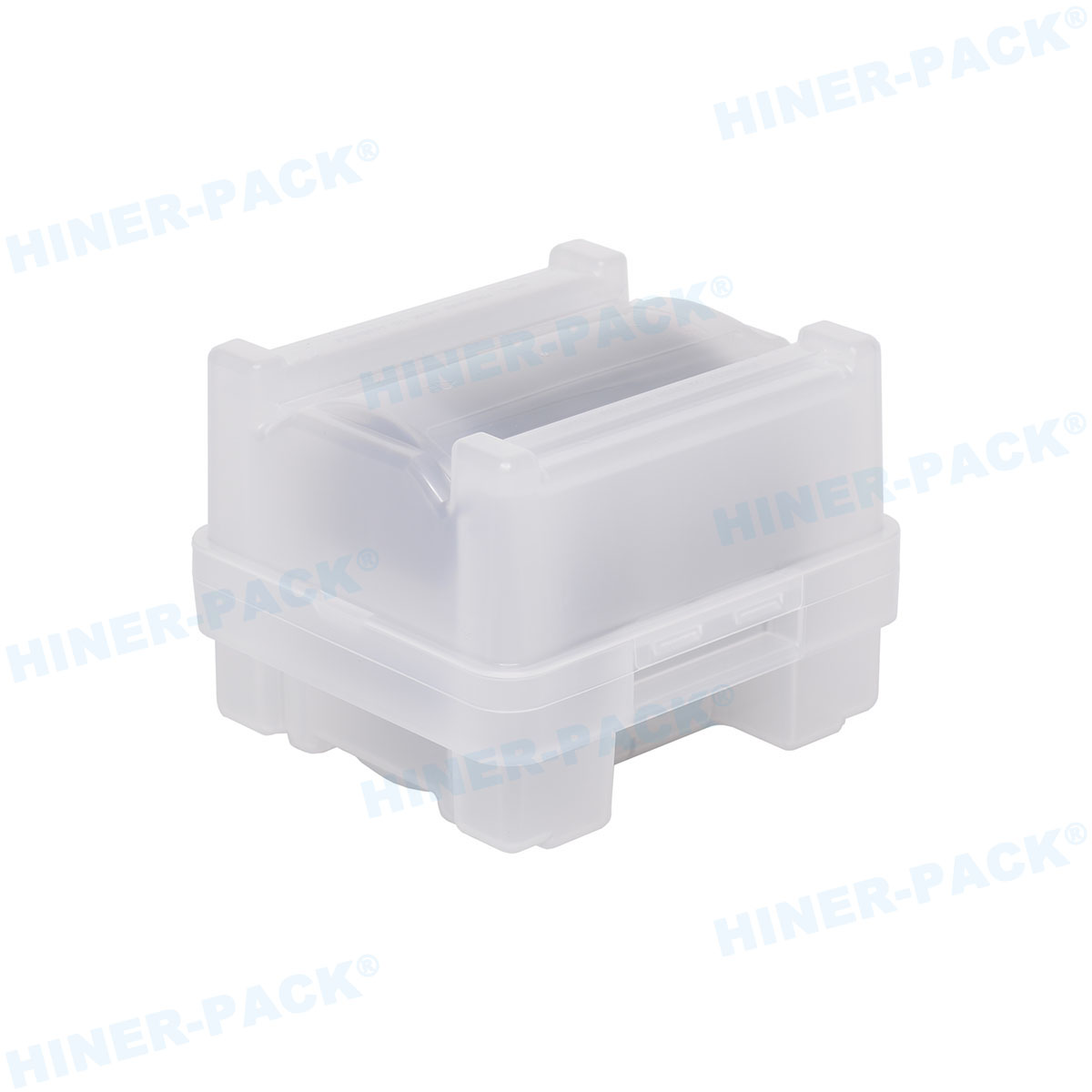
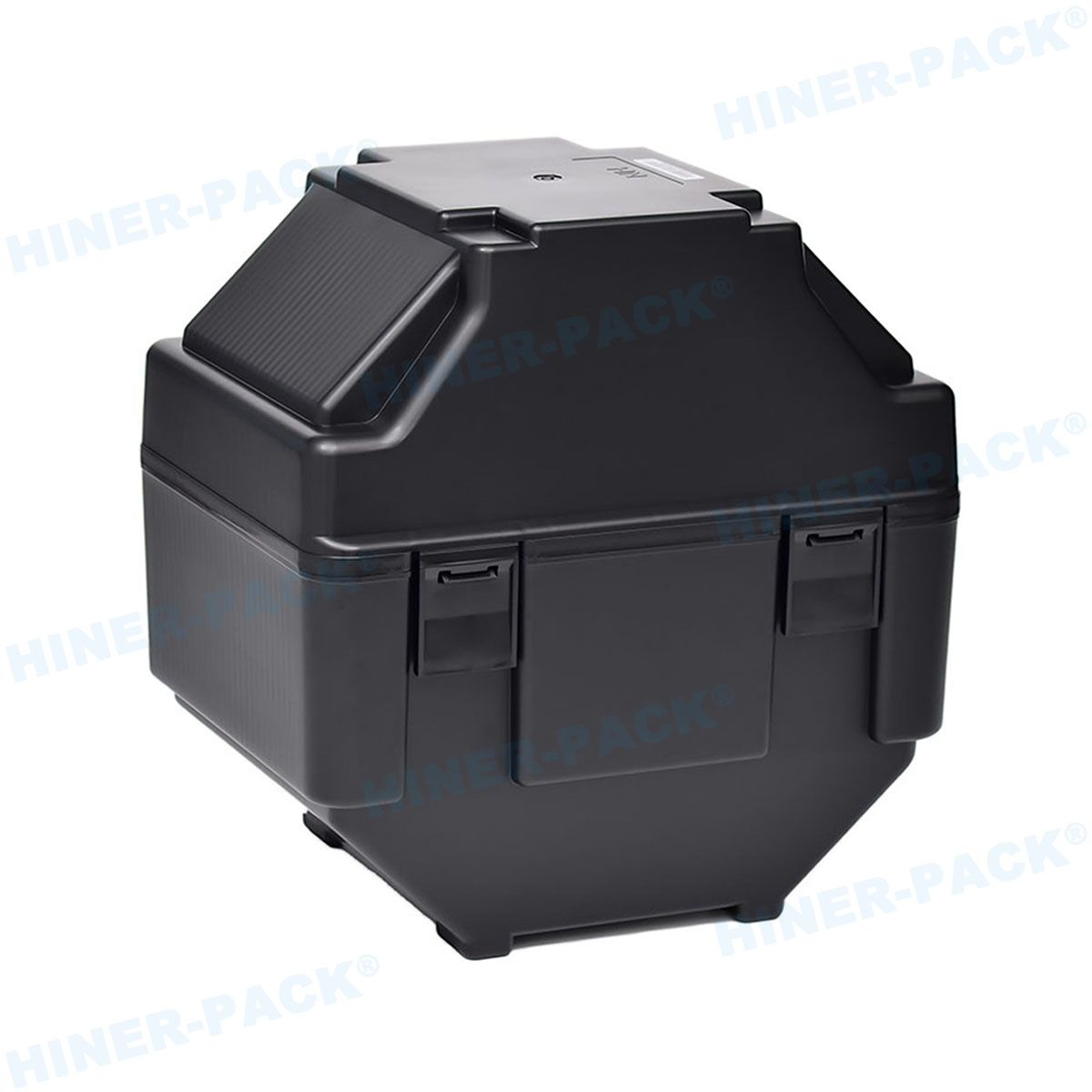
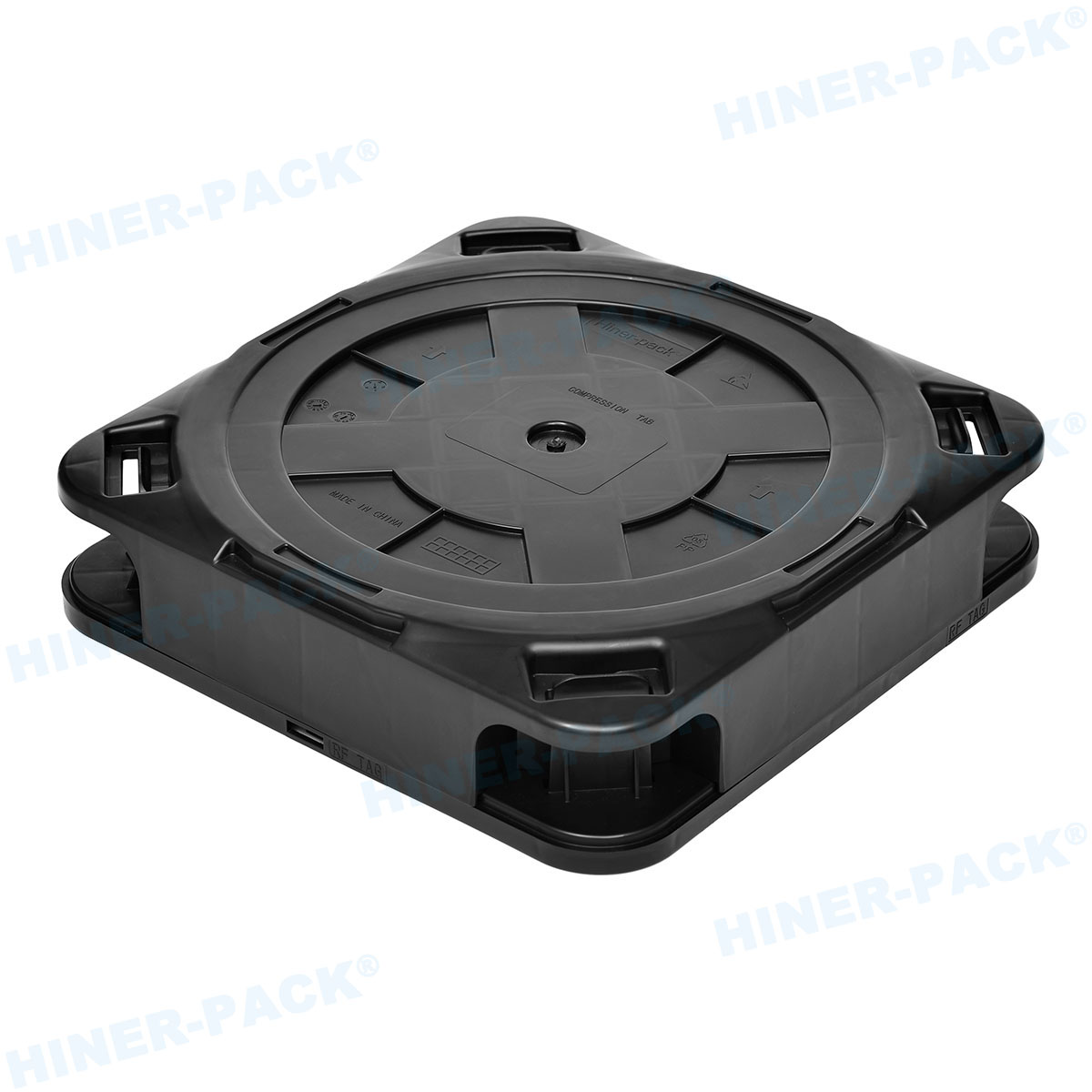
- Wafer Carrier Series
- Wafer Shipper Accessories
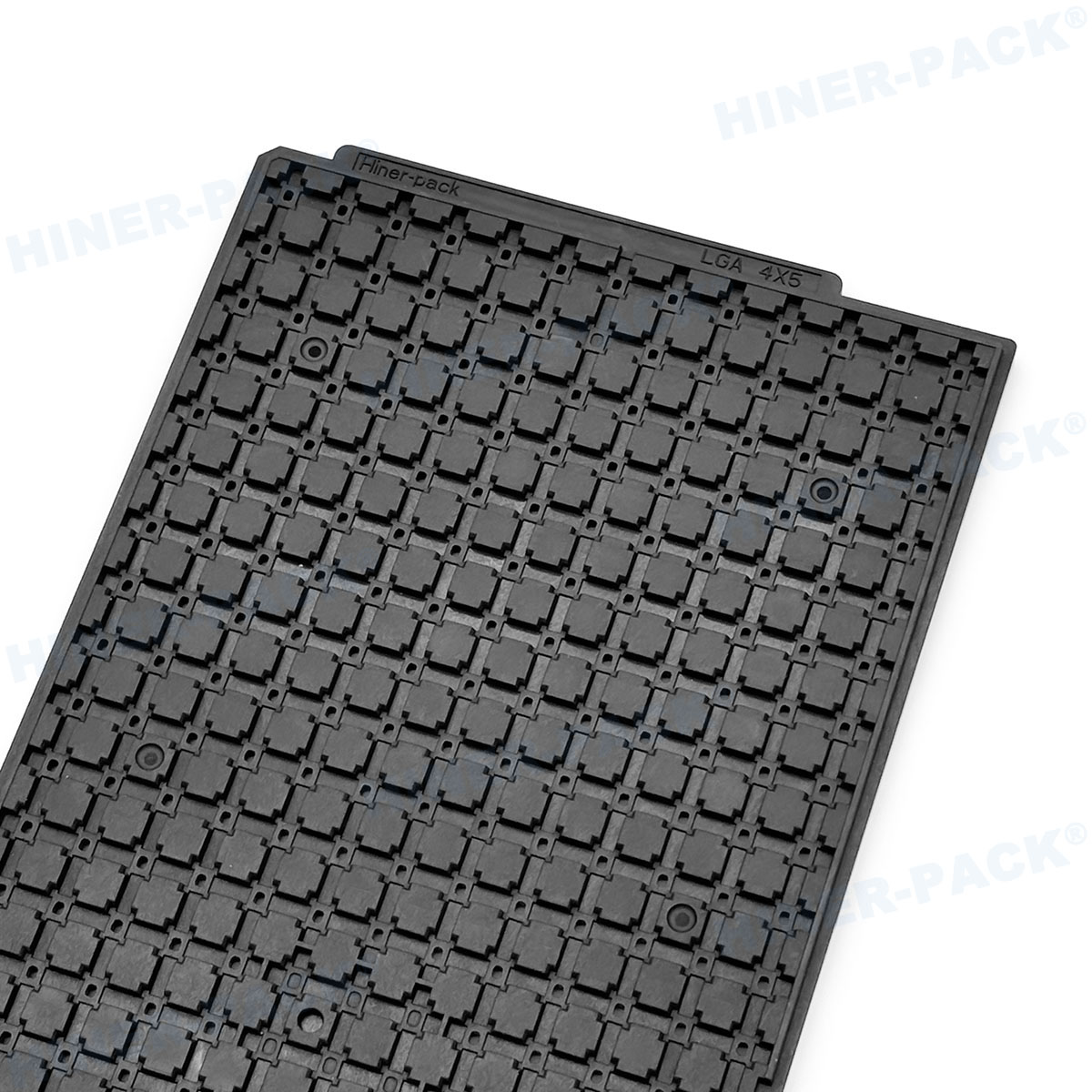
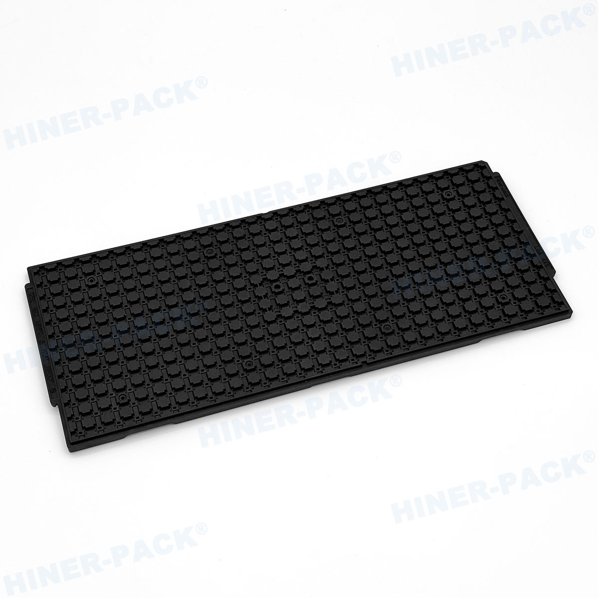
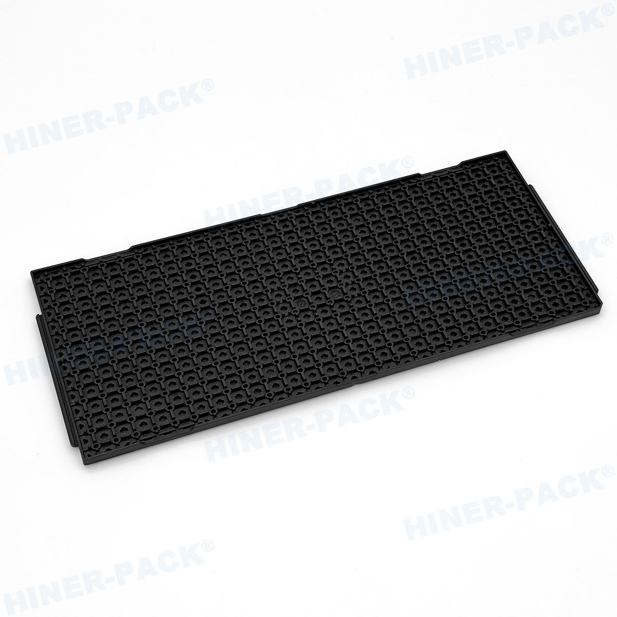
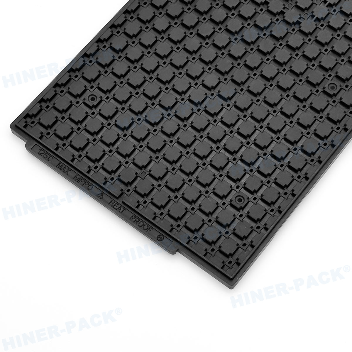
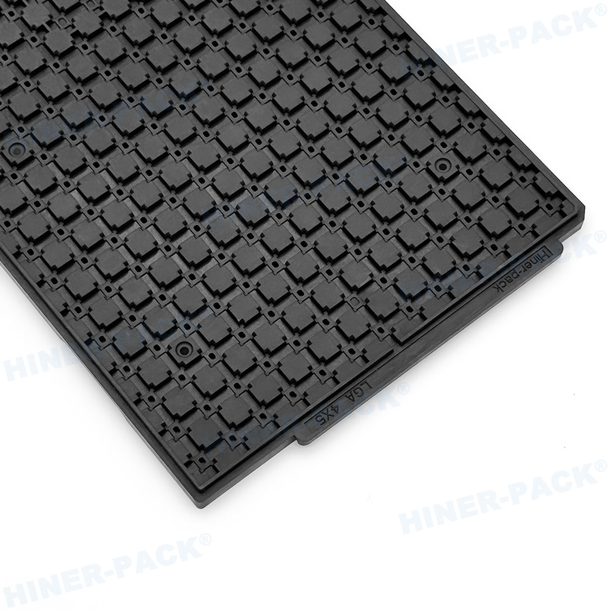
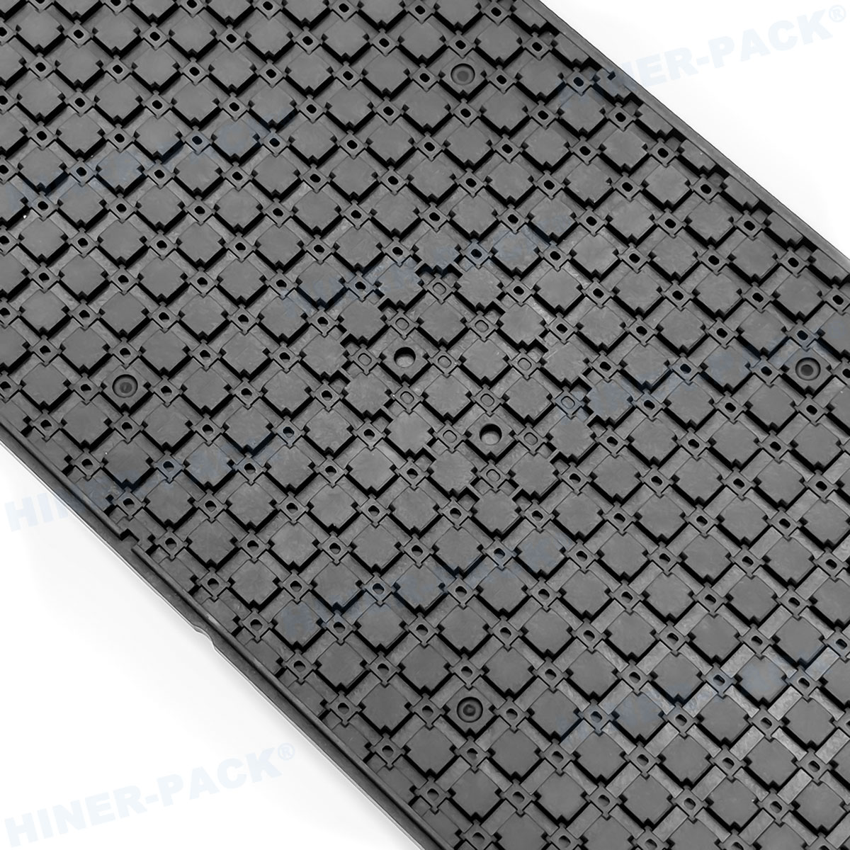
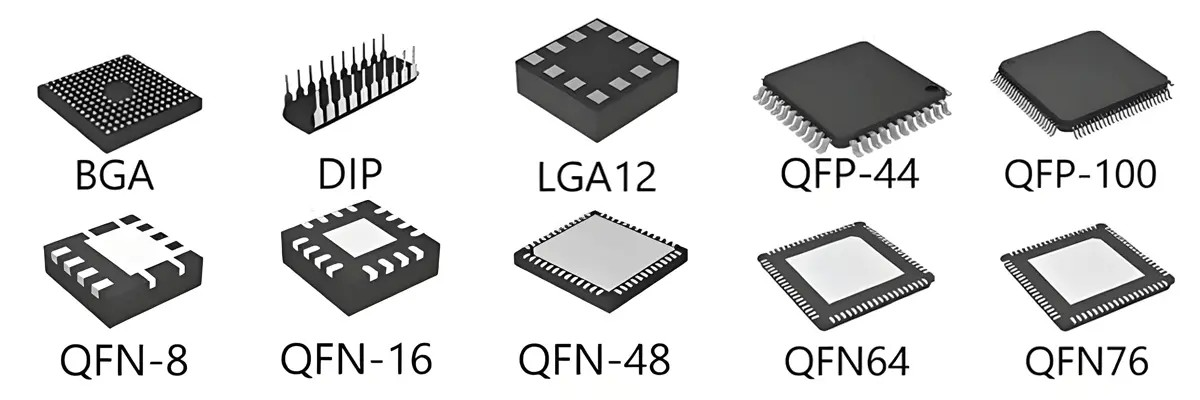
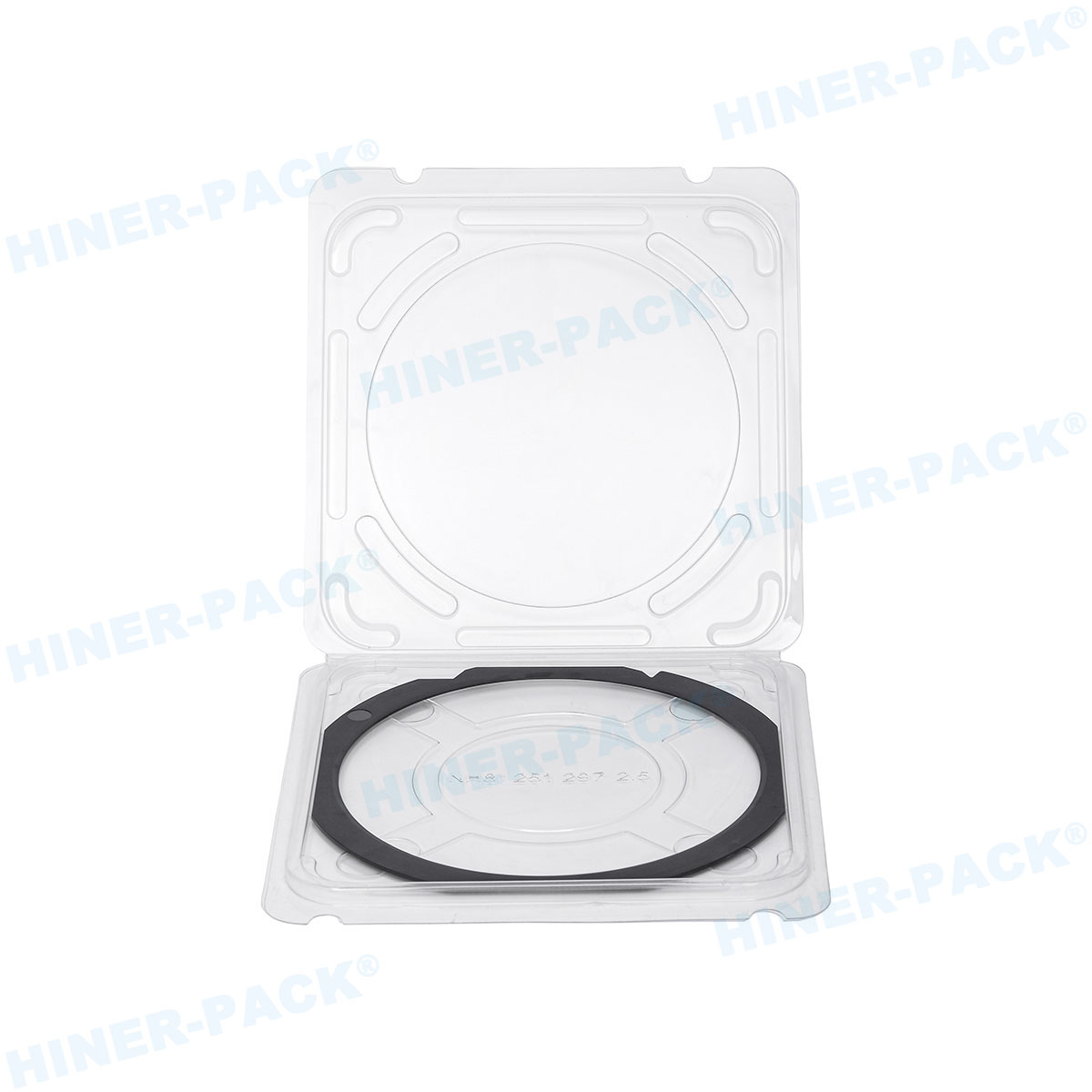
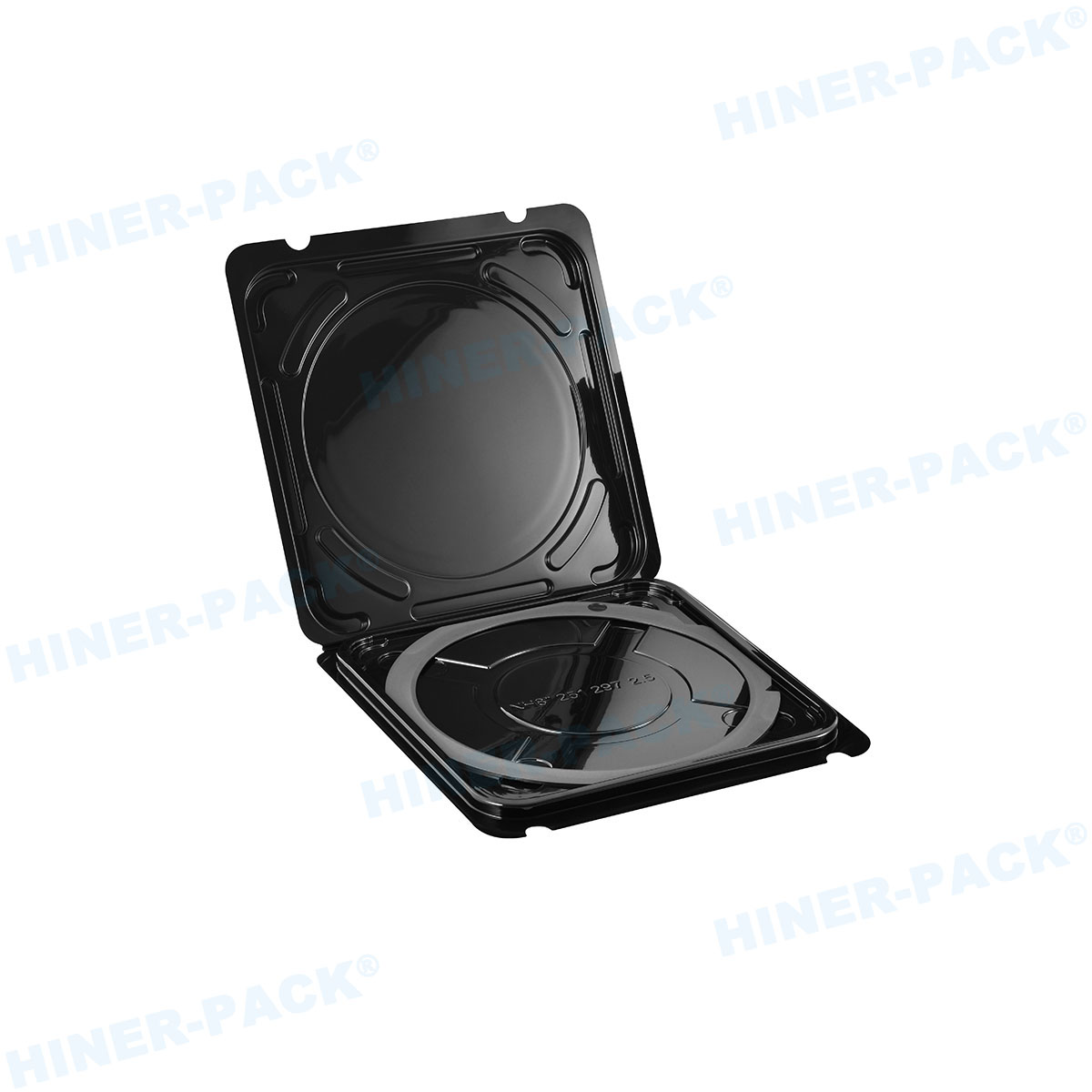
- JEDEC Tray/lC Tray
- Waffle Pack/Chip Tray
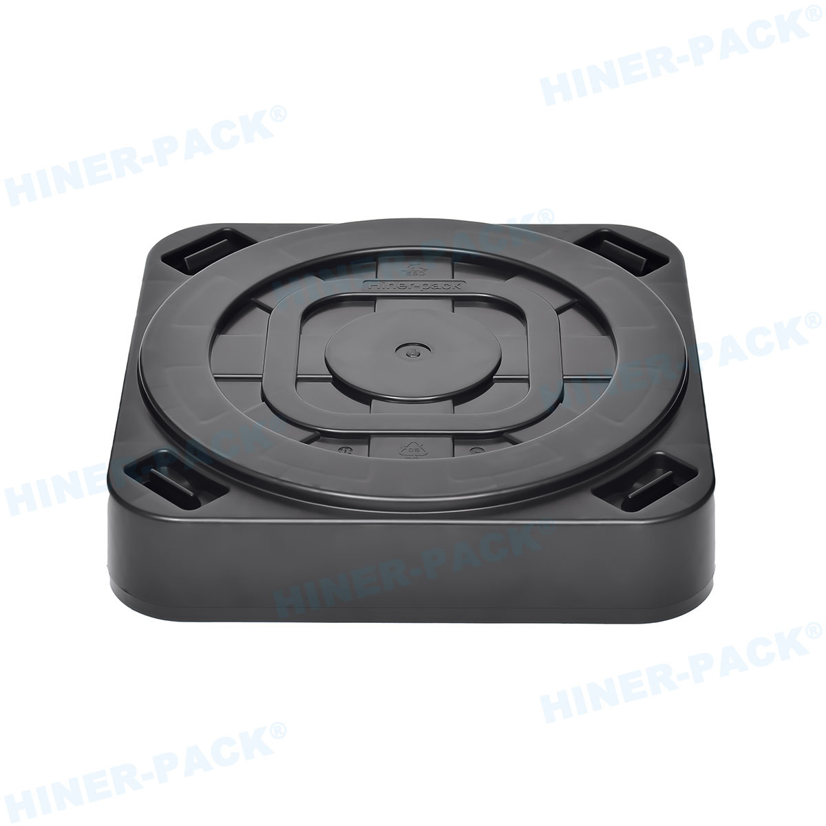
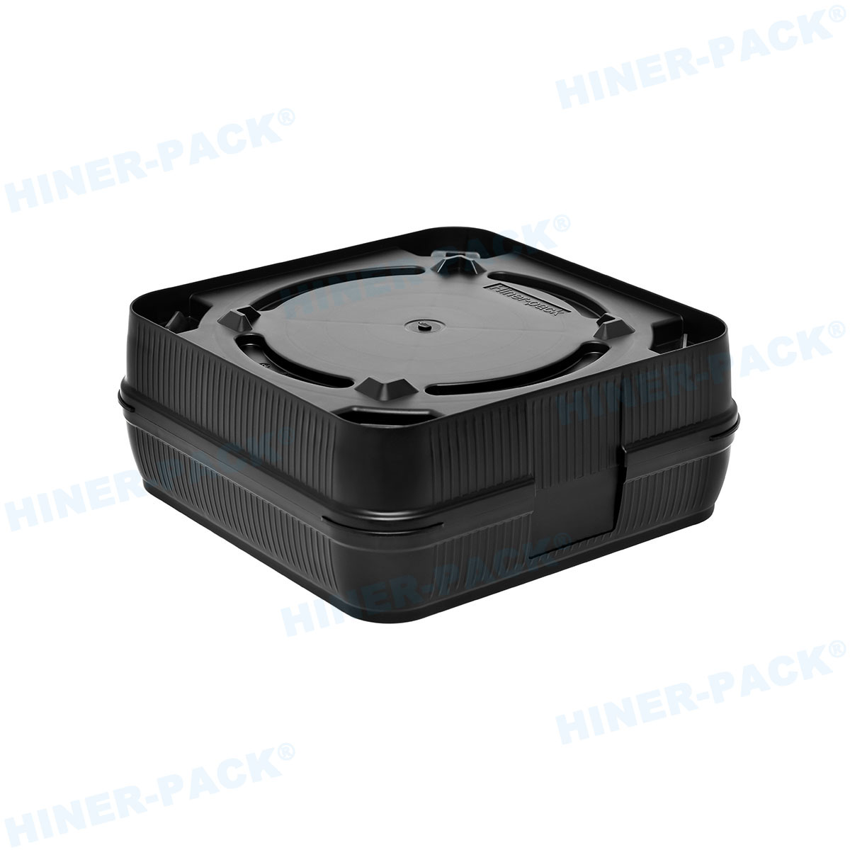
- Gel Box/Vacuum Release Box
- CASES
- NEWS
- DOWNLOADS
- CONTACT US
LANGUAGE