Home > PRODUCTS > JEDEC Tray (thickness 12.19mm)

JEDEC Tray For RFIC

- Absolutely no contact any RF-sensitive surfaces
- Use the body for support to avoid transmitting mechanical/thermal/electrical stress to the RF chip
- The material and structure minimize stray electromagnetic and magnetic contamination and ionic/particulate contamination
- Compatibility with testing, baking, and production line interfaces
- Support non-standard customization

Description

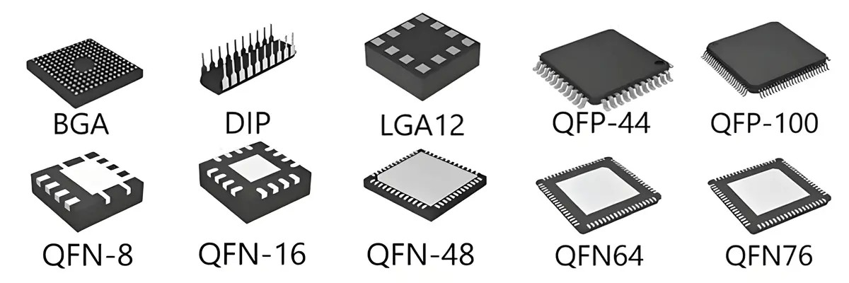
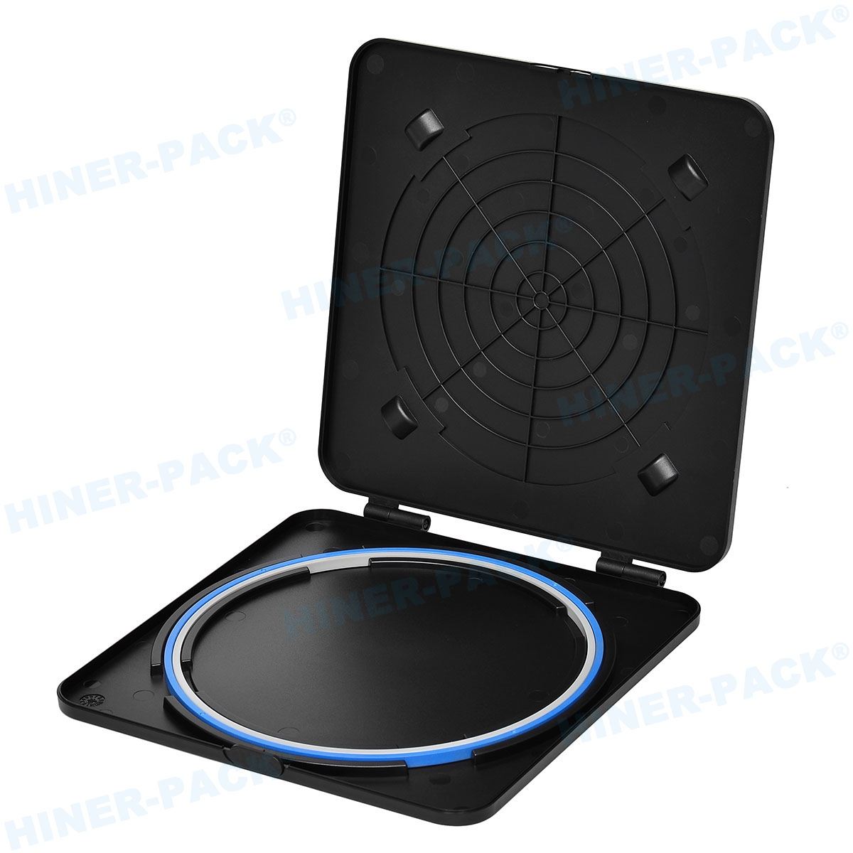
Reference Factors for Designing Trays for RFICs

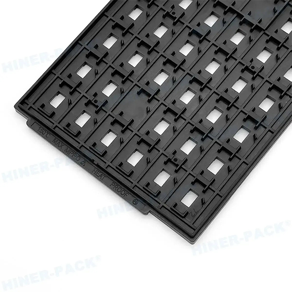
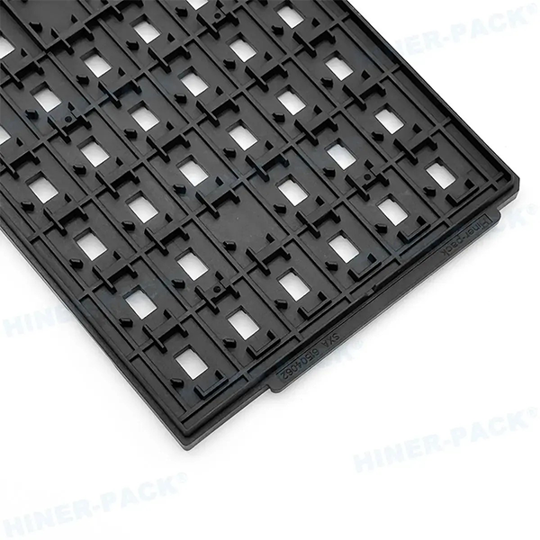
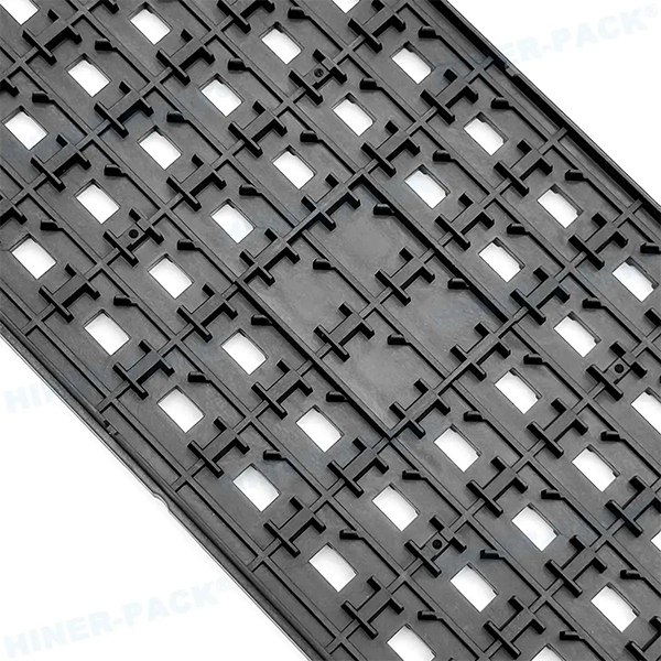
Absolutely do not contact any RF-sensitive surfaces (antenna/output port/exposed die/solder pad/bond-pad).

Use the body for support to avoid transmitting mechanical/thermal/electrical stress to the RF chip.

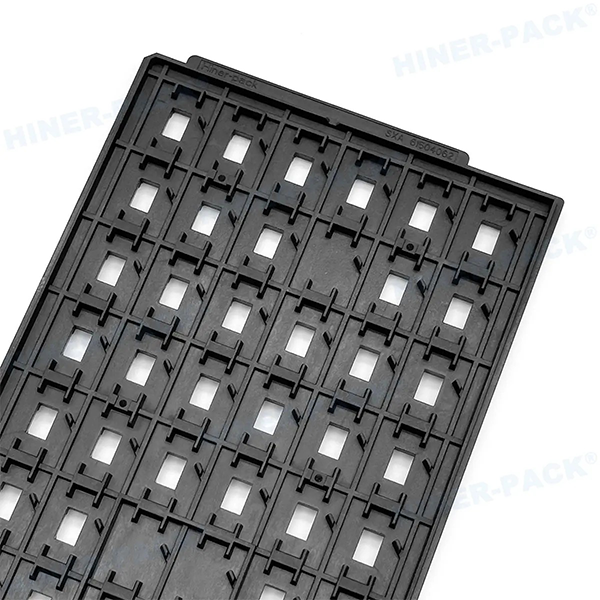
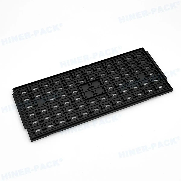
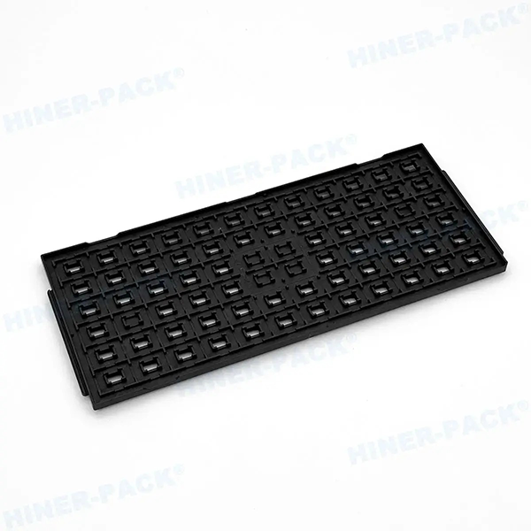
The material and structure should minimize stray electromagnetic and magnetic contamination and ionic/particulate contamination, ensuring compatibility with testing, baking, and production line interfaces.

Meanwhile, ensure that the tray has sufficient mechanical strength to withstand certain pressures and impacts, preventing deformation or damage due to external forces during handling, storage, and automated production processes, thereby protecting the chip from physical damage. The tray's structural design should ensure stable placement of the chip in the tray, avoiding displacement or shaking during movement. Strictly control the tray's dimensional accuracy to ensure precise matching with the chip dimensions, ensuring that the chip can be accurately and stably placed in the designated position on the tray. Additionally, the tray's outer dimensions and structure should be compatible with subsequent production and testing equipment, facilitating automated loading, unloading, and testing processes.

Reference Materials

  • Hiner-pack® JEDEC Tray Catalogue.pdf

    838 kB

Application

Widely used for the packaging, storage, and transportation of IC packages, semiconductor chips, electronic modules, and optical devices.

Specifications

MaterialMPPO, PEI, PES, PPE, ABS, etc.Outline Size (LxWxT)322.6x135.9x12.19mm ("T" is customizable)
Package TypeBGA, DIP, QFN, QFP, LGA, SOP, etc.Cavity SizeCustomizable
ColorBlack, Red, Yellow, Green, White, etc.Cavity QuantityCustomizable
Mold TypeInjection MoldingFlatness/WarpageMAX 0.76mm
Surface Resistance1.0x104~1.0x10¹¹Ω/sqCertificateRoHS
ServiceAccept OEM and ODM
DesignBased on original samples, or custom designs can be created
PackingBy carton or according to customer’s request
SampleSample charge: 1. Free for stock samples
                              2. Custom tray samples to be negotiated
Sample time: After the draft is confirmed and payment is arranged
Lead Time5-7 Working days (The exact lead time depends on the order quantity)


wechat