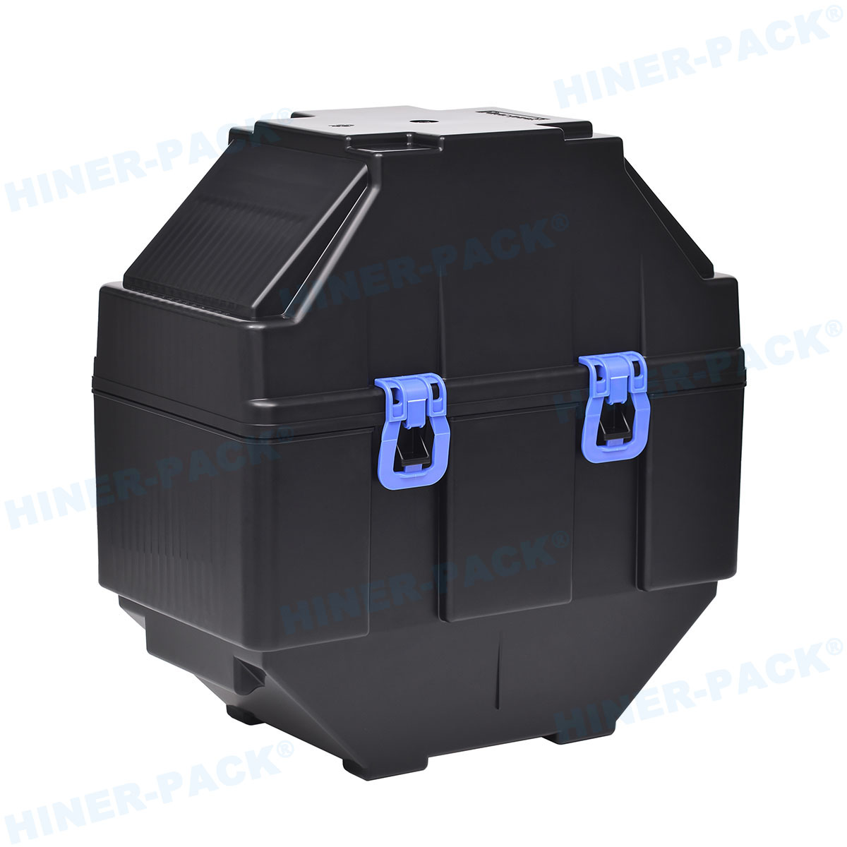
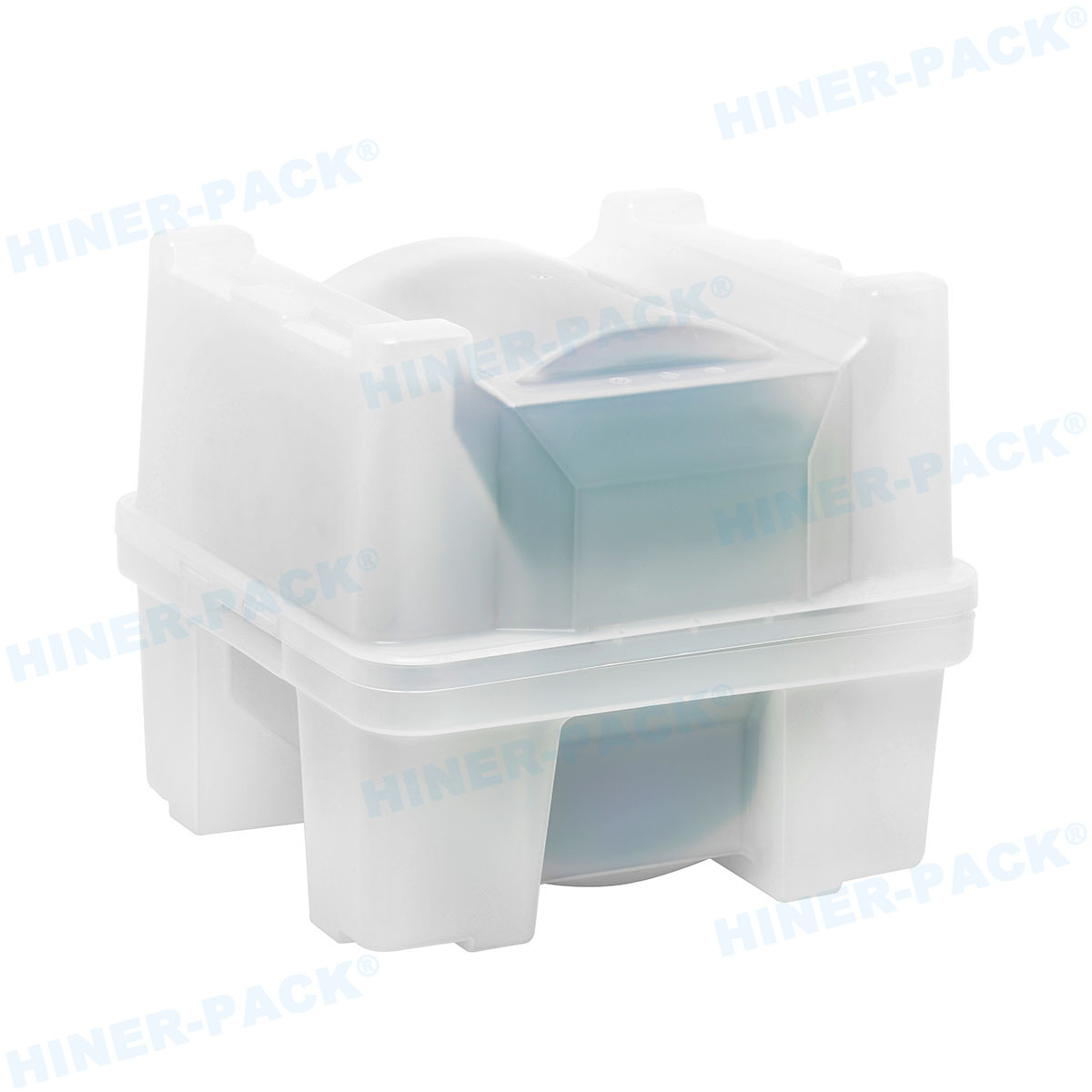
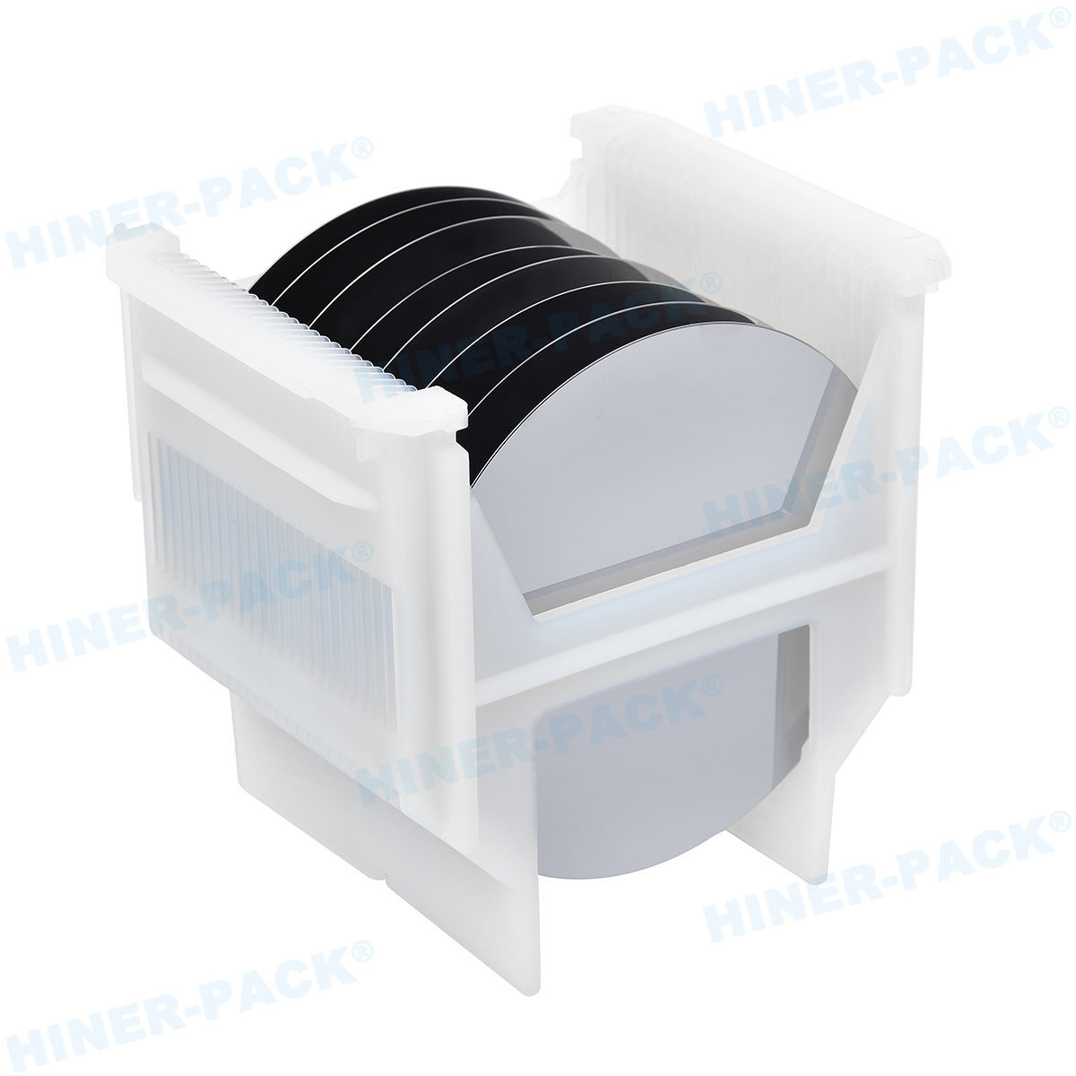
In the rapidly evolving world of semiconductor technology, the 3 inch wafer holds a unique position, bridging historical advancements with modern niche applications. As industries strive for miniaturization and efficiency, understanding the role of the 3 inch wafer becomes crucial for engineers, researchers, and tech enthusiasts alike. This article delves into the multifaceted aspects of the 3 inch wafer, providing a comprehensive overview that highlights its relevance in today's tech landscape. From its basic definition to its manufacturing intricacies, we explore why the inch wafer remains a vital component in various sectors, ensuring you gain a well-rounded perspective on this foundational element.

What is a Inch Wafer?
A 3 inch wafer refers to a thin, disc-shaped slice of semiconductor material, typically silicon, that measures approximately 3 inches (76.2 mm) in diameter. These wafers serve as the substrate for fabricating integrated circuits (ICs), microchips, and other electronic components. The 3 inch wafer emerged during the early days of the semiconductor industry, particularly in the 1970s and 1980s, when it represented a standard size for research and small-scale production. Unlike larger wafers, the 3 inch variant is often associated with legacy systems, educational tools, and specialized applications where cost-effectiveness and flexibility are paramount. The material composition of a 3 inch wafer usually involves high-purity silicon, though other materials like gallium arsenide may be used for specific purposes. Its relatively smaller size allows for easier handling and lower waste in prototyping, making the 3 inch wafer a practical choice for startups and academic institutions. Moreover, the 3 inch wafer has played a pivotal role in the development of early computing devices, laying the groundwork for the advanced technologies we see today. As we move forward, the 3 inch wafer continues to find its place in retrofits and custom solutions, demonstrating its enduring utility in a world dominated by larger formats.
Manufacturing Process of 3 Inch Wafers
The production of a 3 inch wafer involves a series of precise and controlled steps to ensure high quality and performance. It begins with the extraction and purification of raw silicon, which is melted and formed into cylindrical ingots through the Czochralski process. These ingots are then sliced into thin wafers using diamond-edged saws, resulting in the characteristic 3 inch diameter. After slicing, the 3 inch wafer undergoes lapping and polishing to achieve a smooth, defect-free surface, critical for subsequent photolithography processes. During photolithography, patterns are etched onto the 3 inch wafer using light-sensitive chemicals and masks, defining the circuitry for electronic components. Doping and deposition steps follow, where impurities are introduced to modify electrical properties, and thin films are added to enhance functionality. Each 3 inch wafer is subjected to rigorous testing and inspection to detect any defects, ensuring that only those meeting stringent standards proceed to packaging and shipment. The entire manufacturing process for a inch wafer emphasizes precision and scalability, allowing for cost-efficient production runs that cater to low-volume demands. This makes the 3 inch wafer ideal for prototyping and specialized markets, where larger wafers might be overkill. Innovations in automation have further refined the production of the 3 inch wafer, reducing human error and increasing yield rates. Overall, the meticulous process behind the 3 inch wafer underscores its reliability and adaptability in diverse technological contexts.
Applications of 3 Inch Wafers in Modern Technology
The 3 inch wafer finds applications across a wide range of industries, thanks to its versatility and cost-efficiency. In the consumer electronics sector, the 3 inch wafer is used in the production of sensors, diodes, and discrete components for devices like smartphones and wearables. Its smaller size makes the 3 inch wafer suitable for research and development labs, where scientists experiment with new materials and designs without the high costs associated with larger wafers. Additionally, the 3 inch wafer is prevalent in the aerospace and defense industries, where it contributes to the manufacturing of radiation-hardened chips and communication systems that require robust performance in harsh environments. The medical field also benefits from the 3 inch wafer, as it enables the creation of micro-electromechanical systems (MEMS) for diagnostic tools and implantable devices. In education, the 3 inch wafer serves as a hands-on teaching aid for students learning about semiconductor physics and fabrication techniques. The automotive industry leverages the 3 inch wafer for developing control units and sensors that enhance vehicle safety and efficiency. Furthermore, the 3 inch wafer supports the Internet of Things (IoT) ecosystem by facilitating the production of low-power chips for connected devices. As renewable energy technologies advance, the 3 inch wafer plays a role in solar cell research, helping to improve energy conversion rates. This broad applicability highlights how the 3 inch wafer remains relevant, even as larger wafers dominate mass production. By catering to niche and innovative fields, the 3 inch wafer continues to drive progress and inspire new technological breakthroughs.
Advantages and Disadvantages of Using 3 Inch Wafers
When considering the use of a 3 inch wafer, it's essential to weigh its advantages and disadvantages to determine its suitability for specific projects. One of the primary benefits of the 3 inch wafer is its affordability; compared to larger wafers, the 3 inch variant involves lower material and processing costs, making it accessible for small businesses and academic research. The 3 inch wafer also offers greater flexibility in prototyping and low-volume production, allowing for rapid iteration and customization without significant financial investment. Its smaller size reduces waste and simplifies handling, which can lead to higher yields in certain applications. However, the 3 inch wafer has limitations, such as lower throughput compared to larger wafers like the 12 inch versions used in high-volume manufacturing. This can result in higher per-unit costs for mass production, limiting the scalability of projects relying solely on the 3 inch wafer. Additionally, the 3 inch wafer may not support the most advanced node technologies, as industry trends favor larger diameters for cutting-edge chips. Despite these drawbacks, the 3 inch wafer excels in scenarios where cost, time, and specialization are critical factors. For instance, in legacy system maintenance or custom instrument manufacturing, the 3 inch wafer provides a practical solution that balances performance and economics. By understanding these pros and cons, stakeholders can make informed decisions about integrating the 3 inch wafer into their workflows, ensuring optimal outcomes for their specific needs.

Comparison with Other Wafer Sizes
Comparing the 3 inch wafer with other common wafer sizes, such as 6 inch, 8 inch, and 12 inch wafers, reveals distinct differences in terms of capacity, cost, and application scope. The 3 inch wafer, with its 76.2 mm diameter, is significantly smaller than the 12 inch (300 mm) wafer, which is the industry standard for high-volume semiconductor production. This size disparity means that a single 12 inch wafer can host many more chips than a 3 inch wafer, leading to economies of scale that reduce per-chip costs in mass manufacturing. However, the 3 inch wafer outperforms larger counterparts in flexibility and accessibility, particularly for research and development. For example, while a 12 inch wafer requires substantial investment in fabrication facilities, the 3 inch wafer can be processed in smaller, less expensive labs, making it ideal for startups and universities. In terms of material usage, the 3 inch wafer generates less waste during slicing and etching, which aligns with sustainability goals. When it comes to technological advancement, larger wafers like the 8 inch and 12 inch varieties often incorporate newer lithography techniques, but the 3 inch wafer remains relevant for legacy technologies and specialized components. The 6 inch wafer, another intermediate size, offers a middle ground but may not provide the same cost benefits as the 3 inch wafer for low-volume orders. Overall, the choice between a 3 inch wafer and other sizes depends on factors like production volume, budget, and technical requirements. By evaluating these comparisons, businesses can strategically select the appropriate wafer size to meet their objectives, with the 3 inch wafer serving as a valuable option for targeted applications.
Future Trends and Innovations Involving 3 Inch Wafers
The future of the 3 inch wafer is shaped by ongoing innovations and shifting market demands, ensuring its continued relevance in the semiconductor industry. As the Internet of Things (IoT) and edge computing expand, the demand for customized, low-power chips produced on 3 inch wafers is expected to grow, driven by the need for affordable prototyping and small-batch production. Advances in materials science, such as the integration of graphene and other two-dimensional materials, could enhance the performance of devices built on 3 inch wafers, opening new possibilities in flexible electronics and quantum computing. Sustainability trends are also influencing the 3 inch wafer market, with efforts to reduce energy consumption and waste during manufacturing, making the 3 inch wafer an eco-friendlier choice for certain applications. In educational and research institutions, the 3 inch wafer is likely to remain a staple for hands-on training, as it provides a cost-effective platform for experimenting with semiconductor processes. Additionally, the rise of open-source hardware and DIY electronics communities may fuel renewed interest in the 3 inch wafer for hobbyist projects and innovation hubs. Collaborations between industry players and academia could lead to specialized foundries focused on 3 inch wafer production, catering to niche markets that larger fabs overlook. While larger wafers will continue to dominate mass production, the 3 inch wafer's adaptability and historical significance position it as a key enabler of future technological breakthroughs. By staying attuned to these trends, stakeholders can leverage the 3 inch wafer to drive innovation and maintain a competitive edge in a dynamic global landscape.
In summary, the inch wafer is more than just a relic of semiconductor history; it is a dynamic and adaptable component that continues to play a vital role in various technological domains. From its fundamental structure and manufacturing process to its diverse applications and comparative advantages, the 3 inch wafer offers a unique blend of cost-efficiency, flexibility, and specialization. As we look to the future, the 3 inch wafer is poised to support emerging trends in IoT, sustainability, and education, proving that size isn't the only determinant of value in the tech world. By appreciating the multifaceted nature of the 3 inch wafer, industry professionals and enthusiasts can harness its potential to foster innovation and address evolving challenges.
Frequently Asked Questions
Q1: What are the primary uses of a 3 inch wafer in today's industry?
A1: The 3 inch wafer is primarily used in research and development, prototyping, educational settings, and specialized applications such as sensors, MEMS devices, and legacy system components. Its cost-effectiveness and flexibility make it ideal for low-volume production and experimental projects where larger wafers would be impractical or too expensive.
Q2: How does the cost of a 3 inch wafer compare to larger wafer sizes?
A2: The 3 inch wafer is generally more affordable than larger wafers like 8 inch or 12 inch versions due to lower material and processing costs. However, for high-volume manufacturing, the per-unit cost may be higher on a 3 inch wafer because of its smaller size and lower throughput, making it better suited for small-scale or niche markets.
Q3: Can a 3 inch wafer be used for advanced semiconductor nodes?
A3: While the 3 inch wafer can support some advanced technologies, it is often limited compared to larger wafers that are optimized for cutting-edge nodes like 7nm or 5nm processes. The 3 inch wafer is more commonly used for older nodes or specialized applications where extreme miniaturization isn't the primary focus.
Q4: What are the environmental benefits of using 3 inch wafers?
A4: The 3 inch wafer offers environmental benefits such as reduced material waste during production and lower energy consumption in smaller fabrication facilities. Its suitability for low-volume runs also minimizes overproduction, aligning with sustainable practices by decreasing the carbon footprint associated with semiconductor manufacturing.
Q5: Is the 3 inch wafer still being produced, or is it becoming obsolete?
A5: Yes, the 3 inch wafer is still being produced and is not obsolete. It remains in demand for specific applications, including education, research, and custom electronics, where its unique advantages outweigh the benefits of larger wafers. Many suppliers continue to offer 3 inch wafers to cater to these niche markets.

