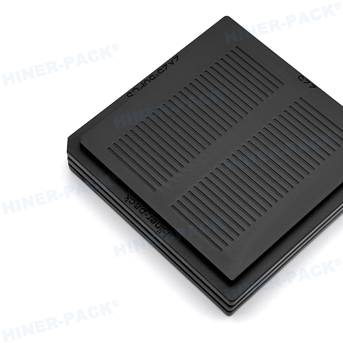
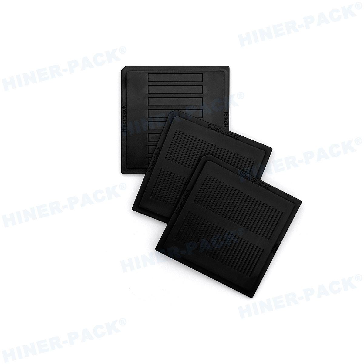
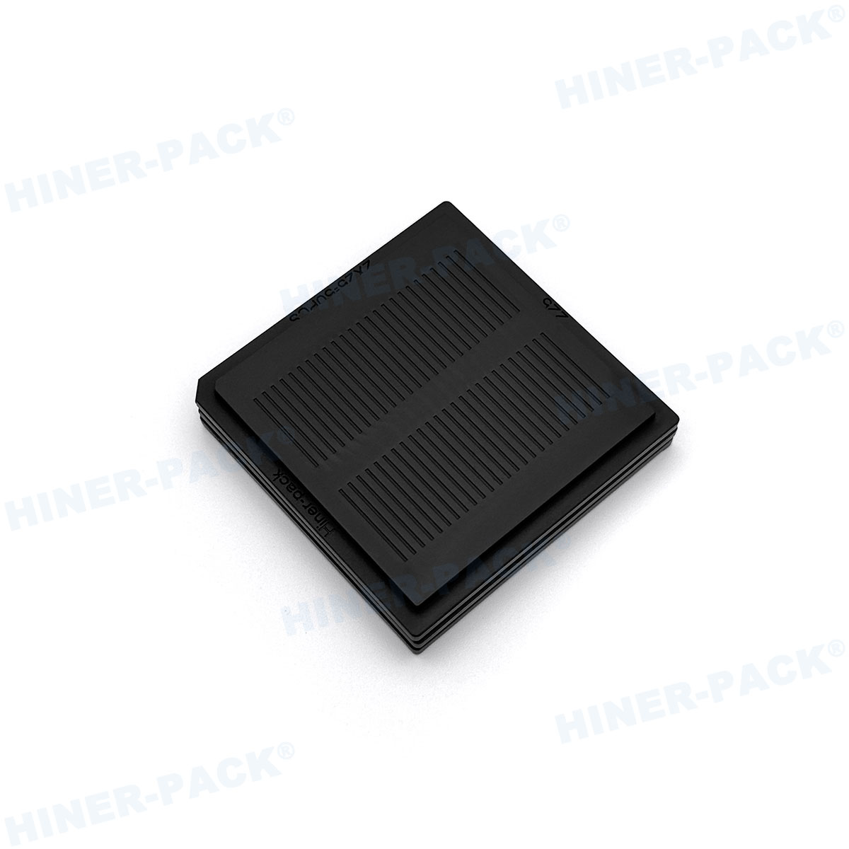
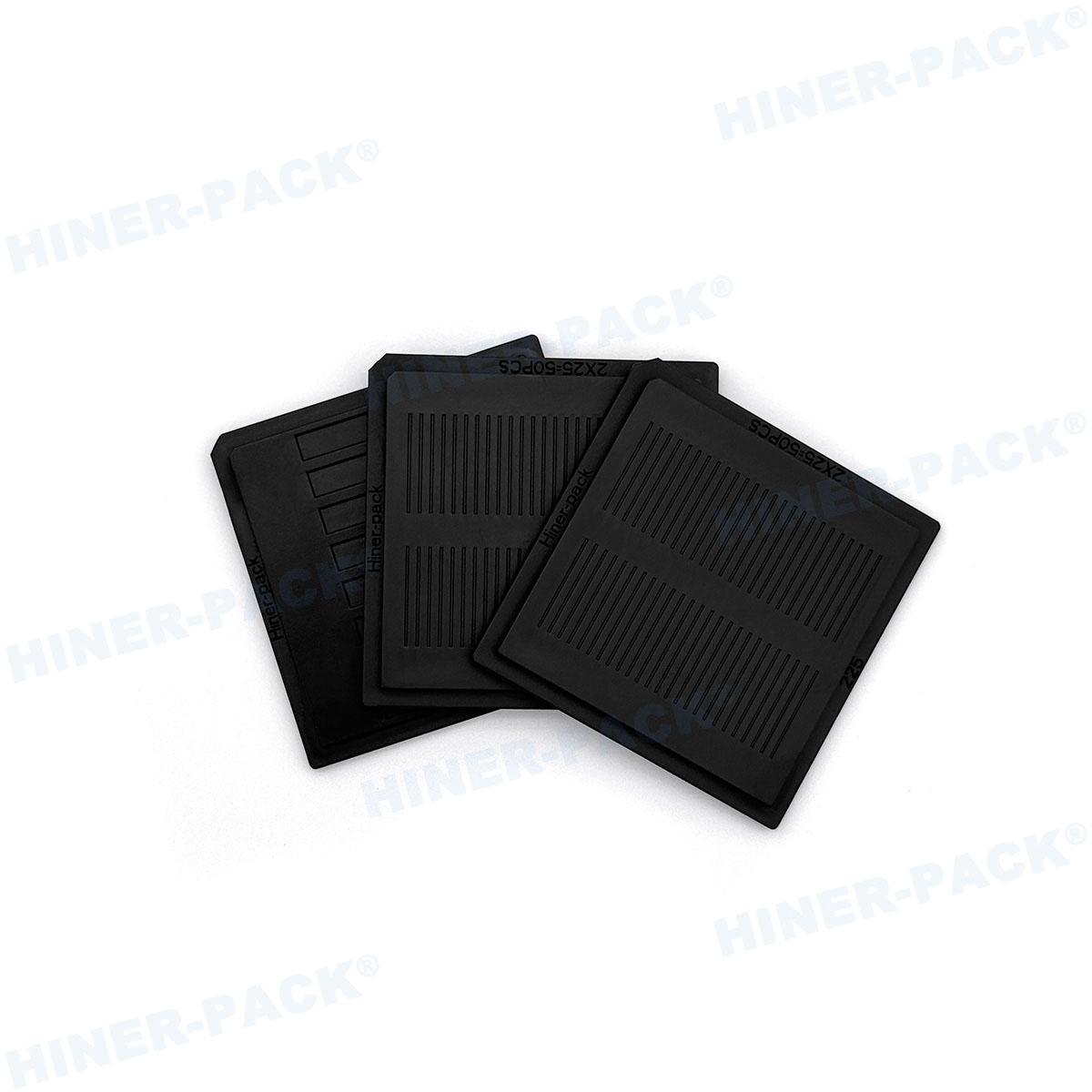
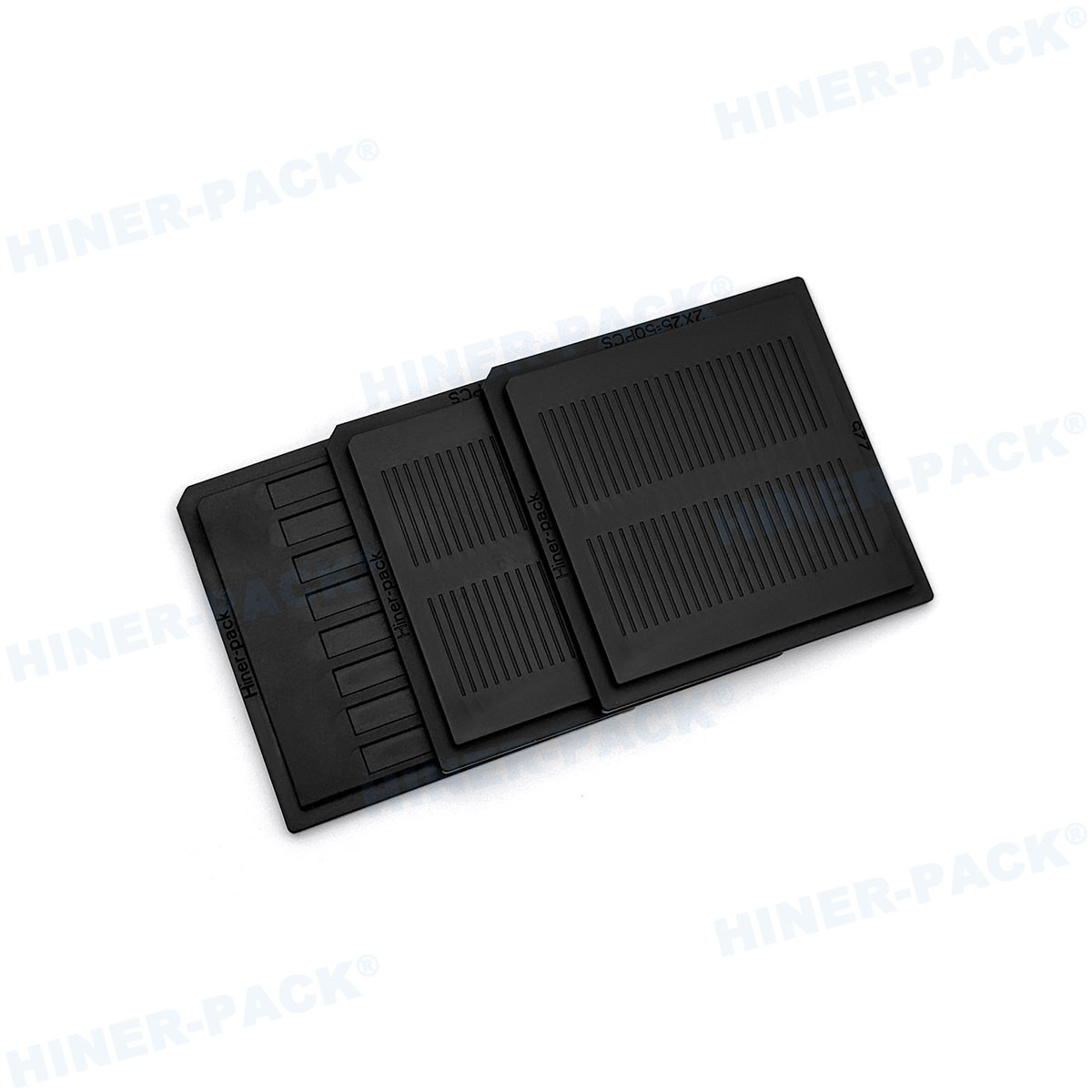
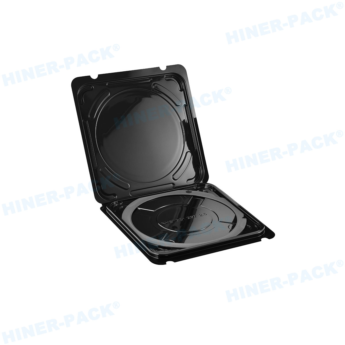
Reference Factors for Designing Bare Die Tray (Waffle Pack)
Avoid any direct pressure or friction on the active surface, bonding pads, or edges of the die: The pocket geometry must fully protect the die without inducing mechanical stress.
Maintain uniform pocket depth and alignment to prevent die tilting, overlap, or edge chipping during loading, transport, or vibration.
Provide antistatic or dissipative properties to control ESD risk throughout assembly, testing, and shipping.
Ensure compatibility with die sorting, pick-and-place, and vision inspection systems commonly used in wafer-level assembly and back-end packaging lines.
Support cleanroom handling requirements: trays should be particulate-controlled, low-outgassing, and chemically stable under typical storage or baking conditions.
Bare Die:
A bare die is an individual semiconductor chip that has been separated (singulated) from the processed wafer but has not yet been packaged or encapsulated. It retains all functional circuitry exposed on its surface, including bonding pads for subsequent wire bonding or flip-chip attachment. Because there is no protective housing, bare die are extremely sensitive to electrostatic discharge, mechanical stress, contamination, and moisture. Their compact size and direct electrical access make them essential for multi-chip modules, system-in-package (SiP) designs, advanced sensor arrays, and prototyping. Handling bare die requires precision tools, particle-controlled environments, and carriers such as waffle packs to prevent edge chipping, pad damage, or orientation loss during inspection, testing, and assembly.