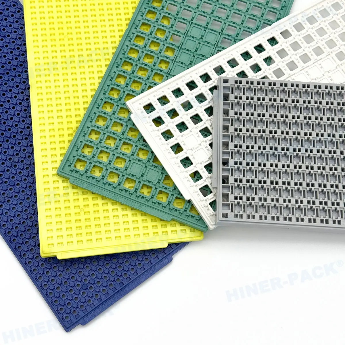
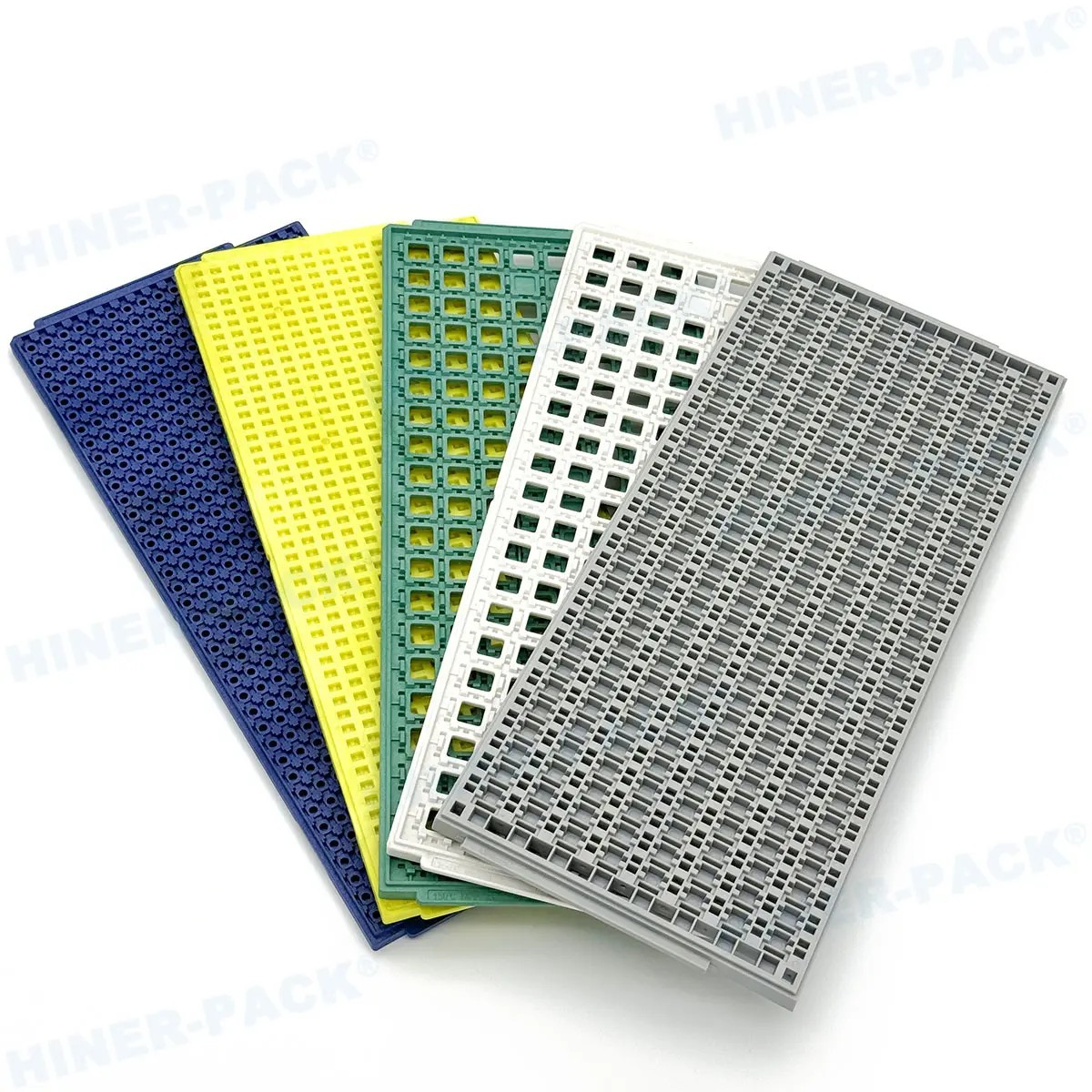
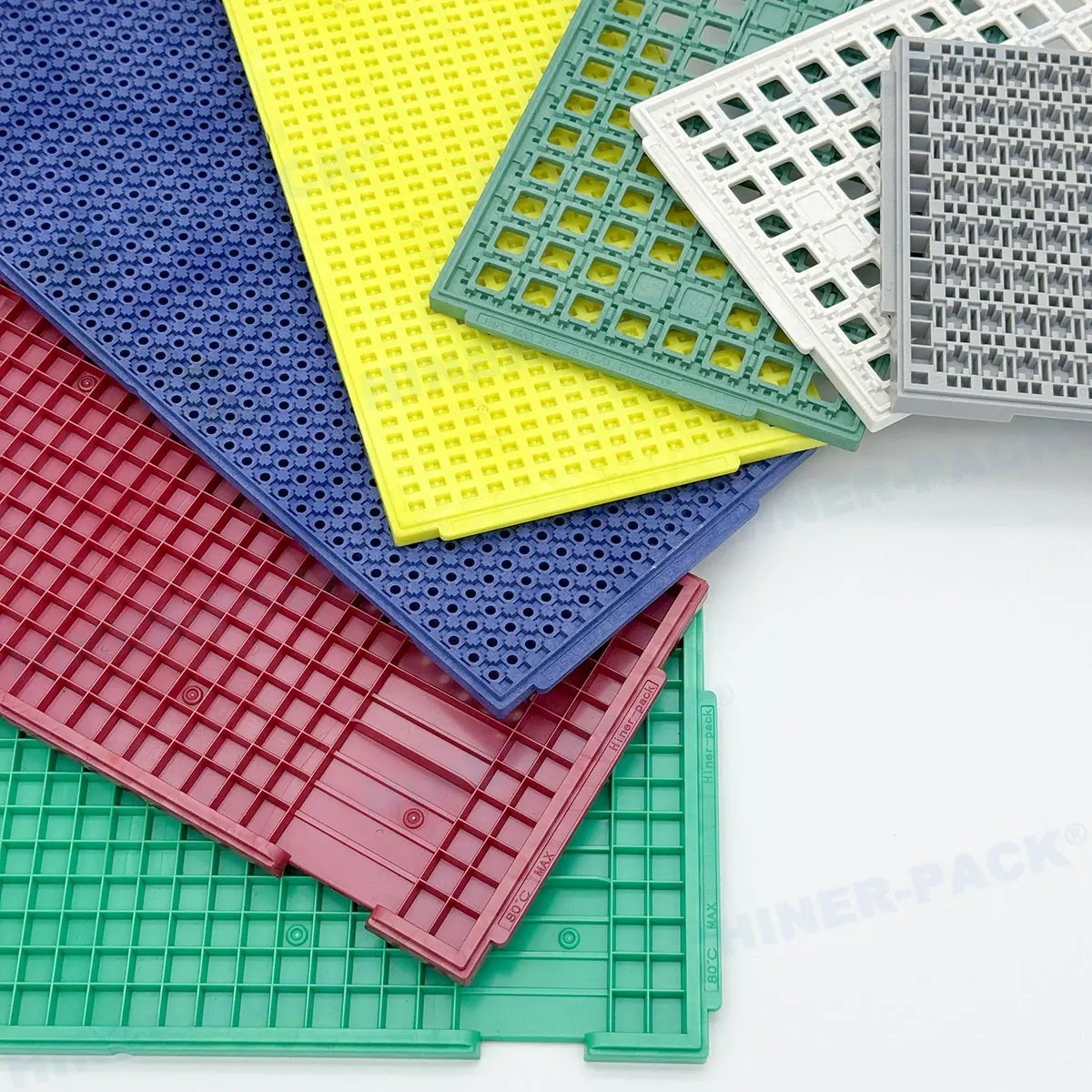
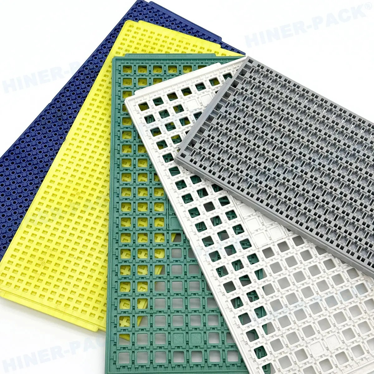
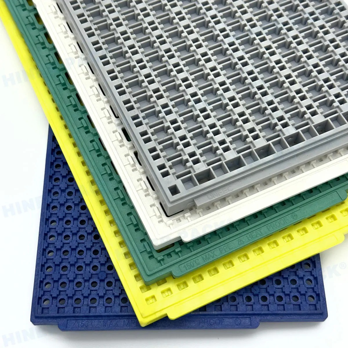
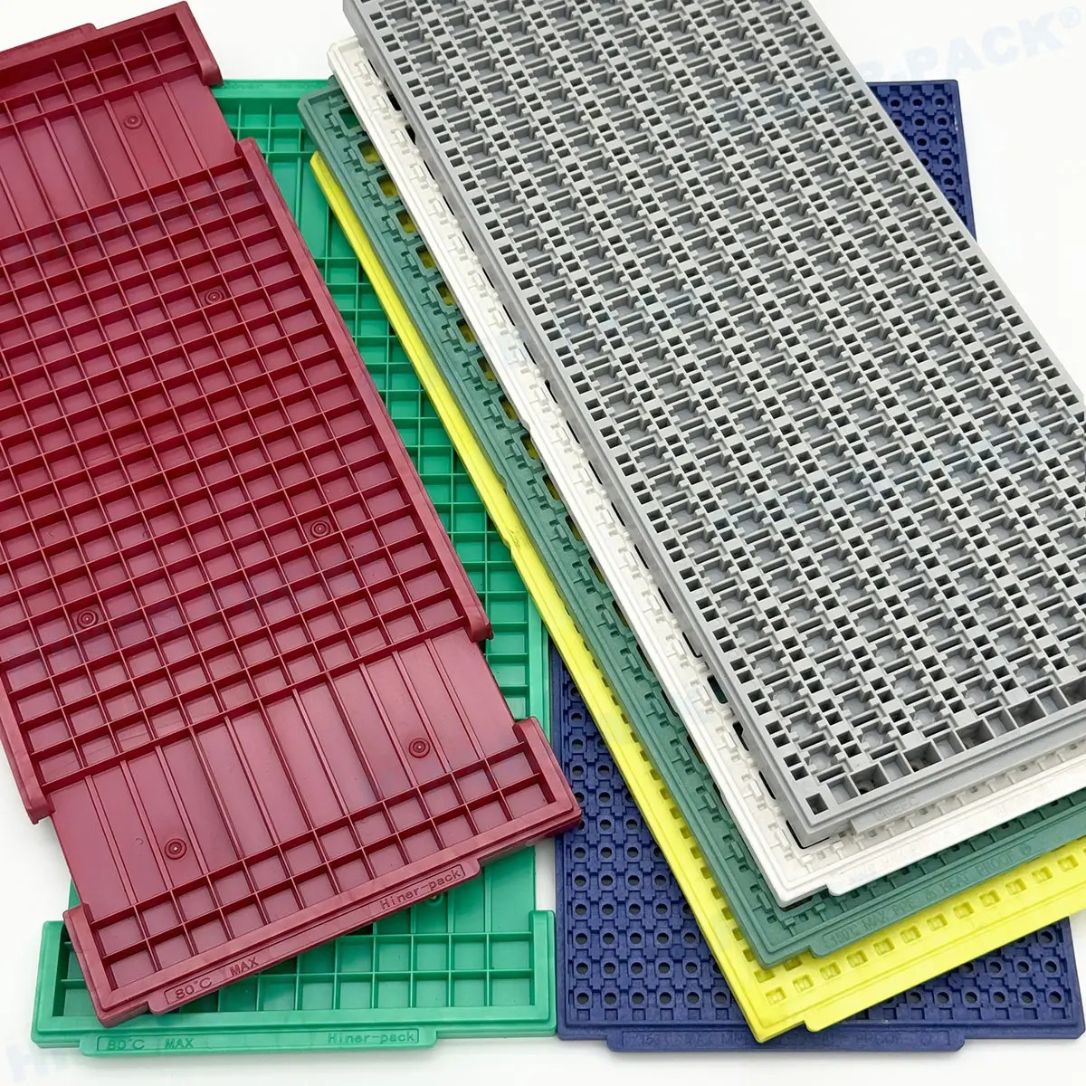
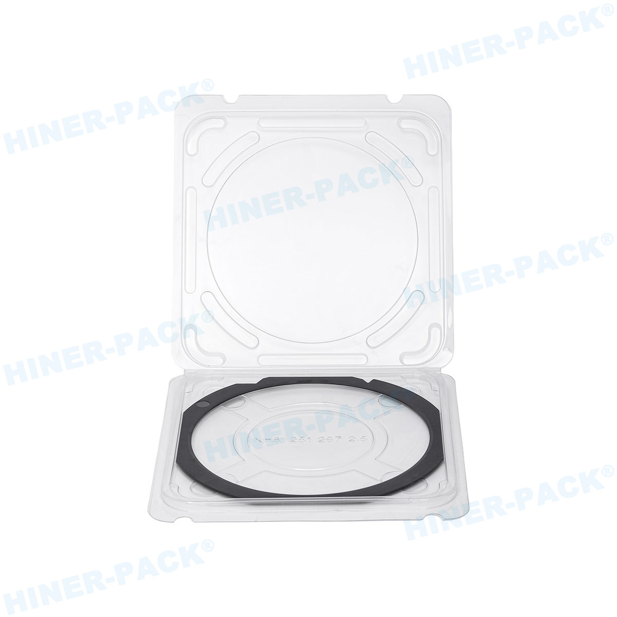
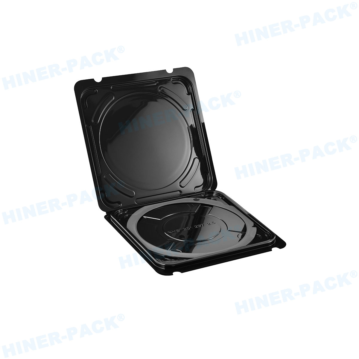
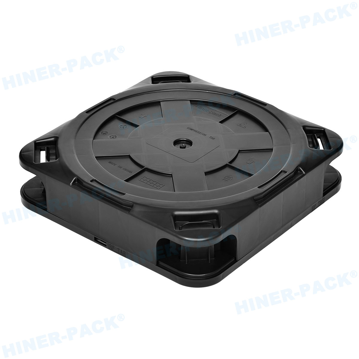
Hiner-pack JEDEC trays are not only designed for reliable semiconductor and electronic component handling but also support full customization in color. Whether you require black, red, green, or other specific colors, customized trays can help with visual management, product differentiation, or branding needs. All trays maintain compliance with JEDEC outline standards, ensuring compatibility with automated handling and pick-and-place systems.
When JEDEC established the matrix tray standard, attention was centered on the external dimensions and defining features, while the interior design was deliberately left open. This decision allowed the tray outline to support a virtually unlimited range of components and applications.
The earliest JEDEC trays were created for the semiconductor industry and are commonly known as IC matrix trays. They remain most widely used in this field, accommodating through-hole devices such as PGA, DIP, and TO packages; surface-mount devices including QFP, BGA, TSOP, and FP packages; as well as leadless packages like LGA, QFN, and LCC. Today, the scope of use has expanded to cover other electronic components—such as connectors, sockets, adapters, PCBs, MEMS, and various small assemblies—streamlining both assembly operations and automated pick-and-place processes.
Beyond electronics, JEDEC outline matrix trays are also applied to non-electronic parts, including lenses, watch components, precision metal pieces, and even synthetic stones, enabling them to be handled with standardized automation equipment.