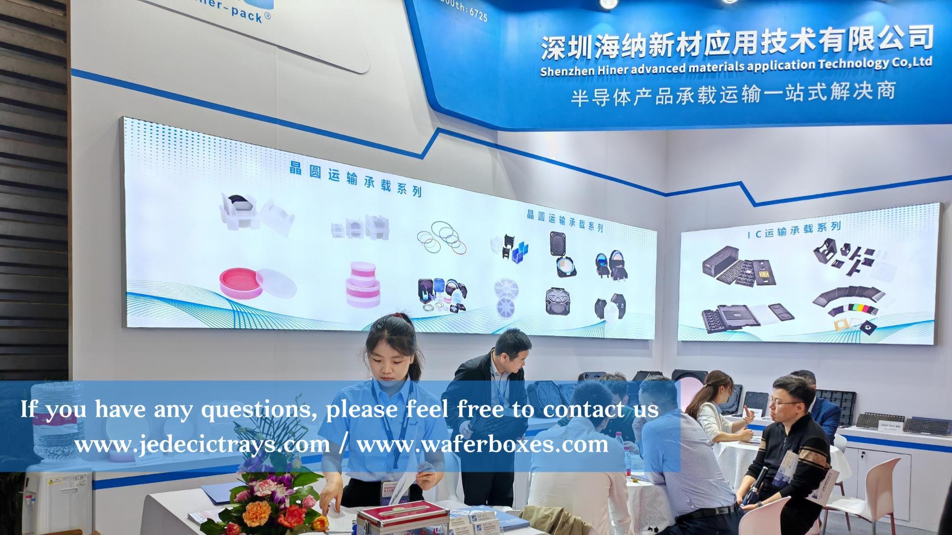
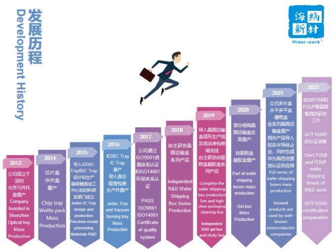
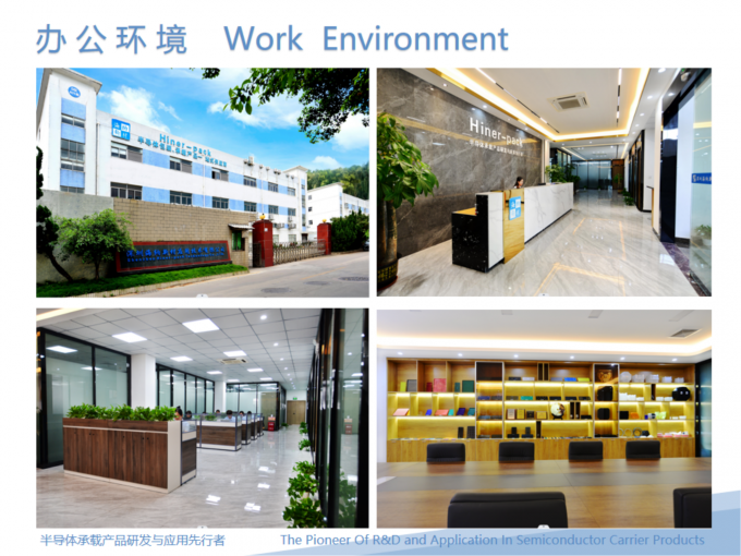
Hiner-pack® was founded in 2013. It is a comprehensive one-stop supplier integrating the design, manufacturing, and sales of automated handling, carrying, and shipping products used for the safe transport and protection of semiconductor wafers and IC chips during fabrication, packaging, and testing stages.
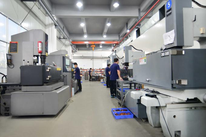
Hiner-pack is equipped with advanced mold processing and injection molding facilities, a high-standard cleanroom cleaning line, and a wide range of testing equipment. We have established close partnerships with many well-known enterprises and jointly set up polymer material R&D bases with domestic universities and research institutes. Through years of development, we have mastered specialized processing techniques and manufacturing capabilities for semiconductor packaging raw materials. We also hold multiple invention and utility model patents. Through persistent efforts, we have built a professional team for material R&D and product design. This enables us to continuously optimize semiconductor packaging solutions and launch new products that meet customers’ high standards of quality.