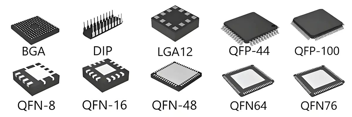
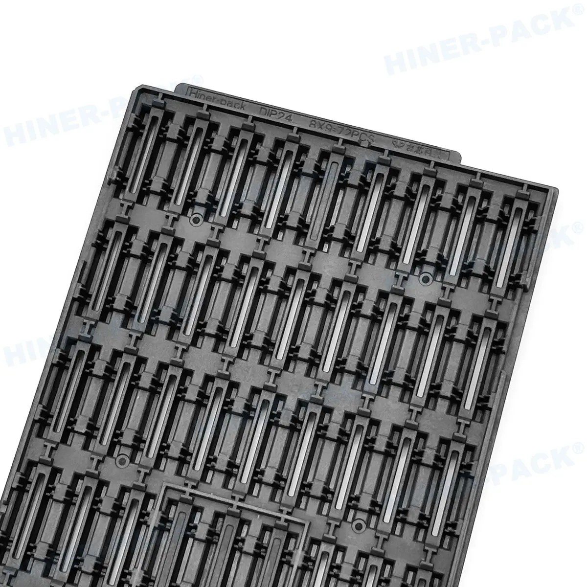
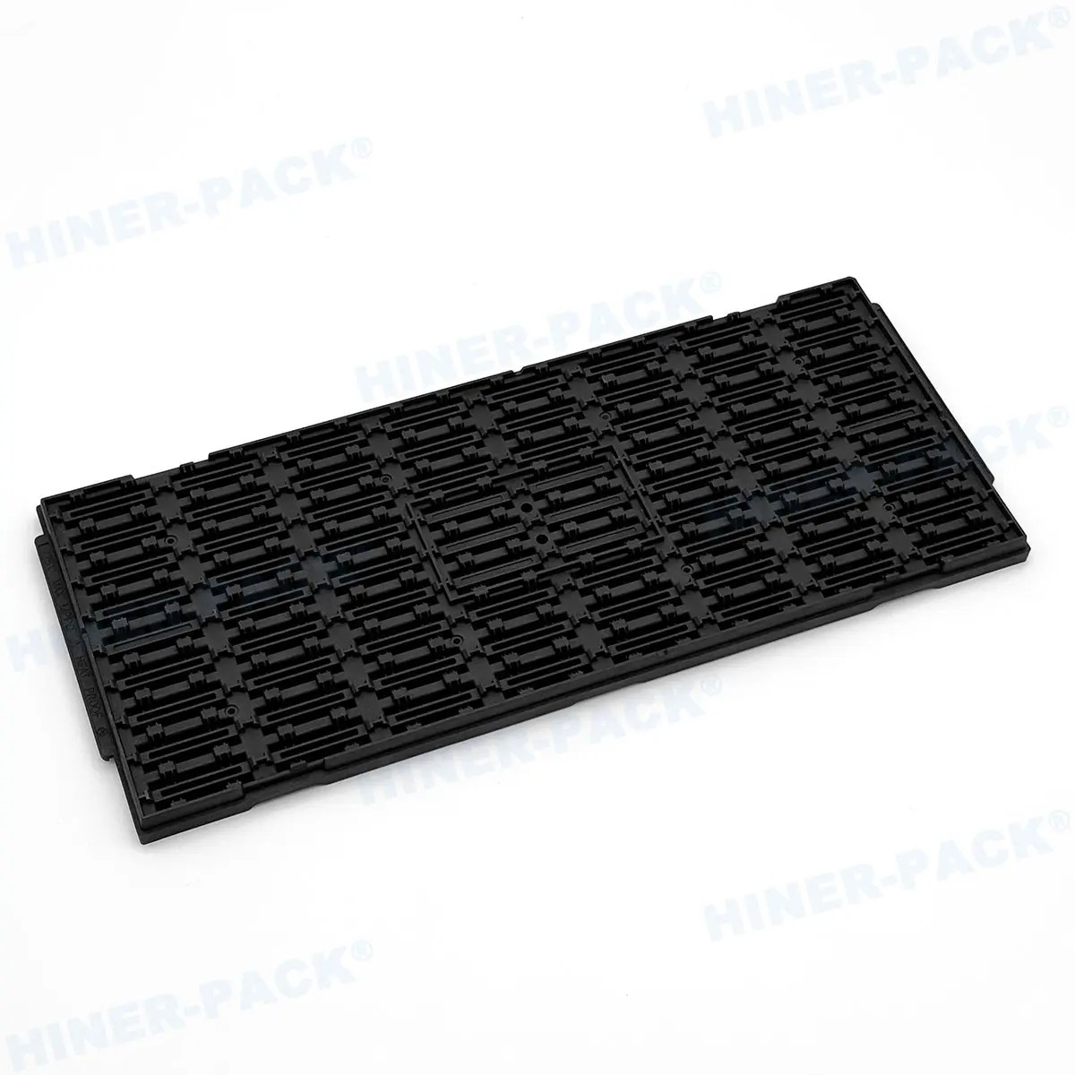
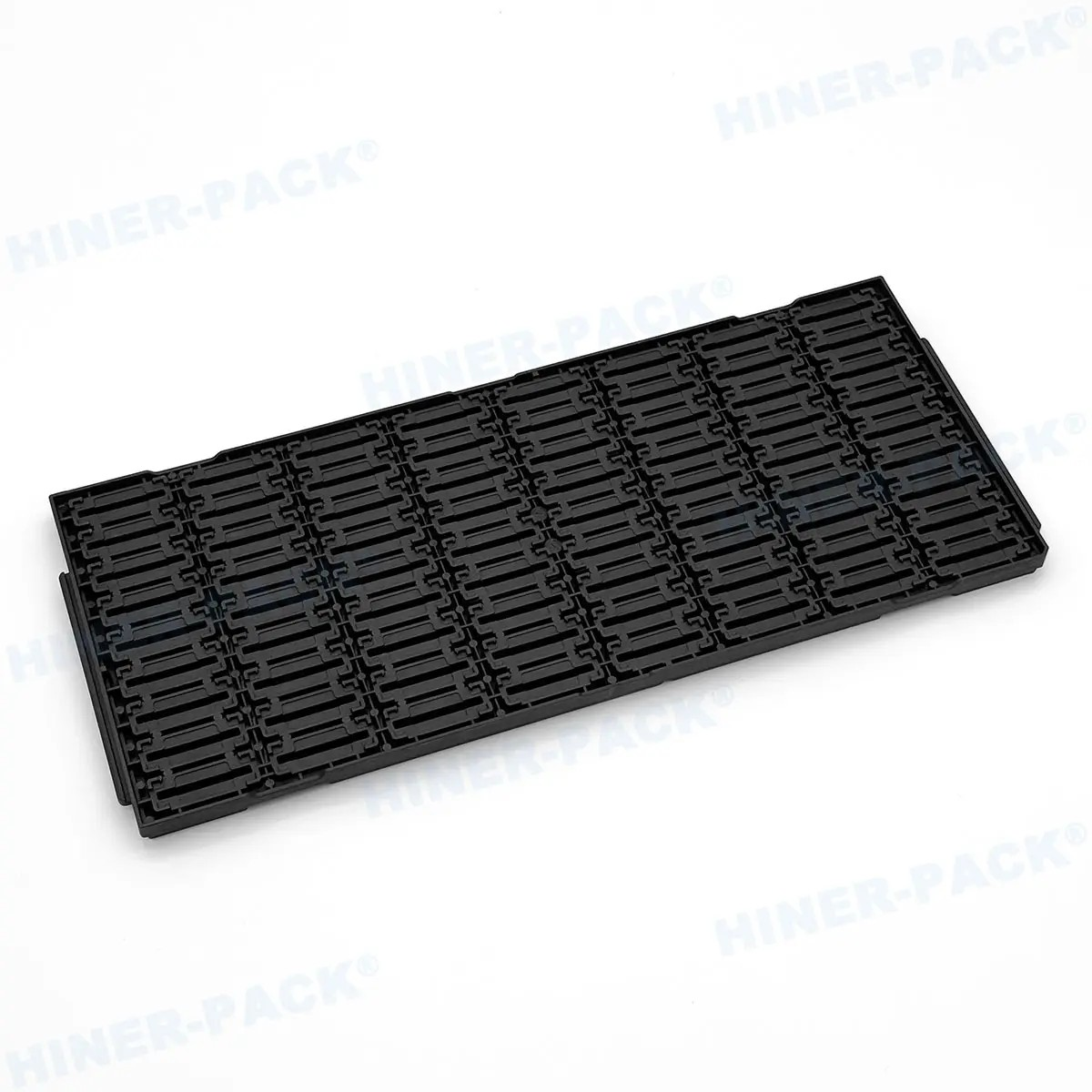
Reference Factors for Designing JEDEC TRAYs Compatible with DIP Packaging
Absolutely do not contact or compress the leads: Any positioning/supporting surface of the tray should support the chip body rather than the leads.
Maintain the integrity of lead shape and spacing: prevent bending, scratching, or plastic deformation.
Ensure compatibility with upstream and downstream equipment (picking and placing, vision, baking, sorting, testing) and meet ESD and cleanliness requirements.
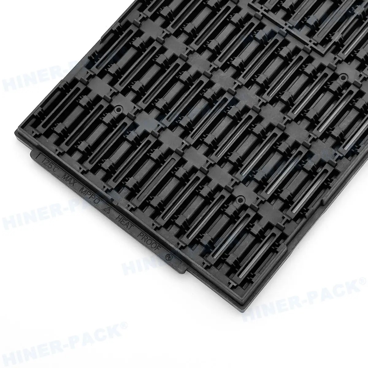
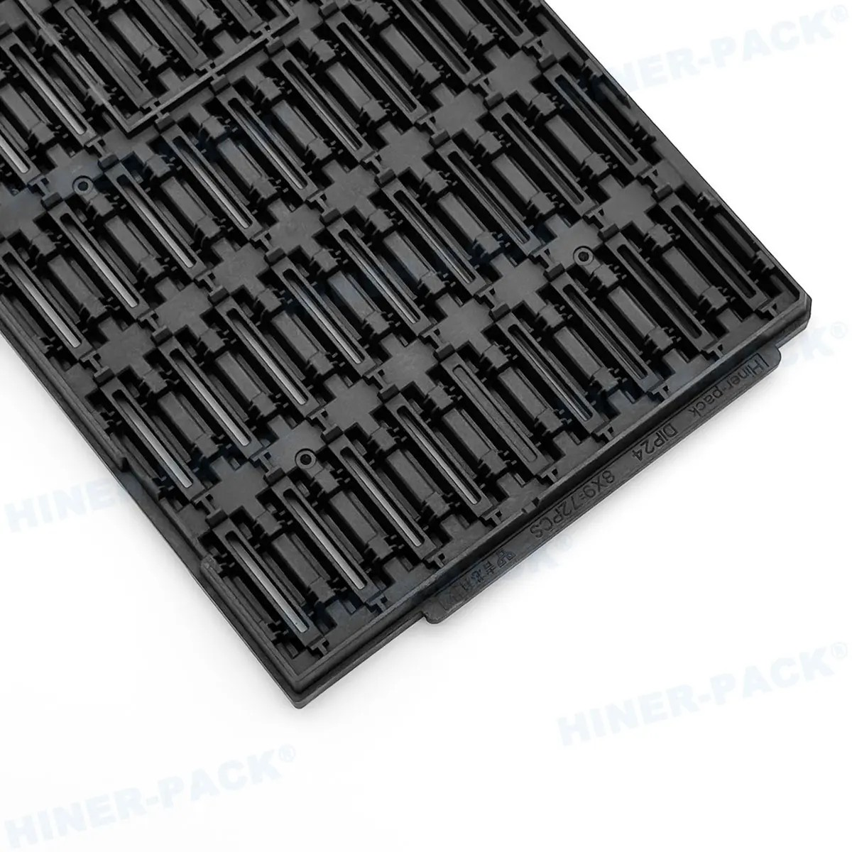
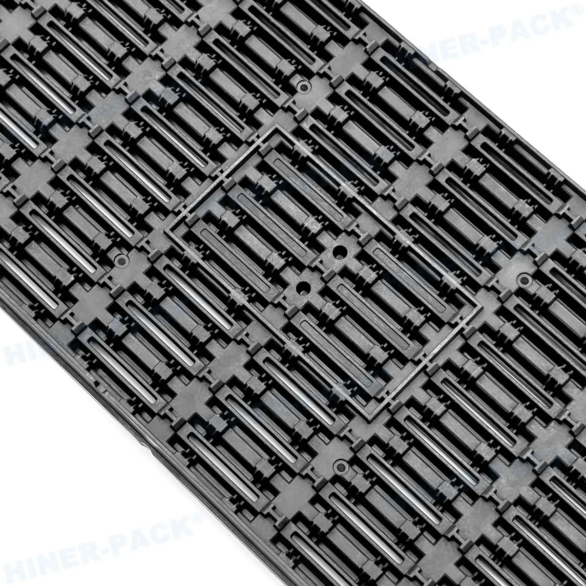
Dual In-line Package (DIP):
DIP is a long-standing through-hole package with leads extending vertically from both sides of the package in a double-row arrangement, needing to be inserted into chip sockets with a DIP structure or directly into PCB through-holes for soldering. It is suitable for through-hole soldering on PCBs, offering convenient operation, mature processing, and ease of maintenance and replacement.
Widely used for the packaging, storage, and transportation of IC packages, semiconductor chips, electronic modules, and optical devices.
Material | MPPO, PEI, PES, PPE, ABS, etc. | Outline Size (LxWxT) | 322.6x135.9x12.19mm ("T" is customizable) |
Package Type | BGA, DIP, QFN, QFP, LGA, SOP, etc. | Cavity Size | Customizable |
Color | Black, Red, Yellow, Green, White, etc. | Cavity Quantity | Customizable |
Mold Type | Injection Molding | Flatness/Warpage | MAX 0.76mm |
Surface Resistance | 1.0x10⁴~1.0x10¹¹Ω/sq | Certificate | RoHS |
Service | Accept OEM and ODM | ||
Design | Based on original samples, or custom designs can be created | ||
Packing | By carton or according to customer’s request | ||
Sample | Sample charge: 1. Free for stock samples 2. Custom tray samples to be negotiated Sample time: After the draft is confirmed and payment is arranged | ||
Lead Time | 5-7 Working days (The exact lead time depends on the order quantity) |