In the fast-paced world of semiconductor manufacturing, precision and efficiency are paramount. Among the many components that ensure smooth operations, the 2 inch wafer carrier plays a crucial role. This specialized container is designed to hold, protect, and transport 2-inch wafers—the foundational substrates for producing microchips, sensors, and other electronic devices. As industries push for miniaturization and higher yields, understanding the nuances of the 2 inch wafer carrier becomes essential for engineers, technicians, and procurement specialists. This article delves into the key aspects of these carriers, highlighting their design, applications, and benefits, while addressing common questions to help you optimize your processes.
What is a 2-Inch Wafer Carrier?
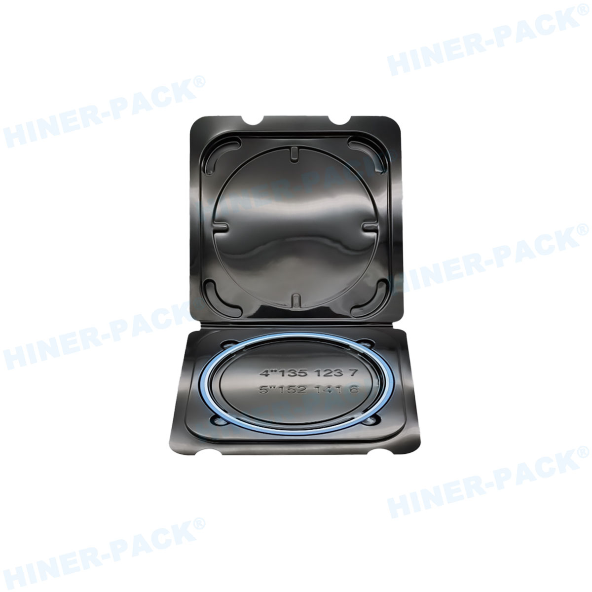
A 2 inch wafer carrier is a protective enclosure specifically engineered to handle 2-inch diameter silicon wafers during various stages of semiconductor fabrication. These wafers are thin slices of semiconductor material used in the production of integrated circuits and other microdevices. The carrier serves as a safeguard against physical damage, contamination, and electrostatic discharge, which could compromise the integrity of the delicate wafers. Typically constructed from high-purity materials, the 2 inch wafer carrier ensures that wafers remain in a controlled environment from cleaning and coating to etching and inspection. Its design often includes slots or grooves that securely hold each wafer in place, preventing movement during transit or processing. This foundational tool is indispensable in labs and production facilities where even minor errors can lead to significant financial losses.
The evolution of the 2 inch wafer carrier mirrors advancements in semiconductor technology. Originally, simpler containers were used, but today's versions incorporate features like RFID tagging and compatibility with automated systems. This makes the 2 inch wafer carrier not just a storage unit, but an integral part of smart manufacturing workflows. By maintaining wafer orientation and minimizing handling, these carriers contribute to higher throughput and reduced defect rates. In essence, the 2 inch wafer carrier is a unsung hero in the semiconductor ecosystem, enabling the precision required for modern electronics.
Design and Materials of 2-Inch Wafer Carriers
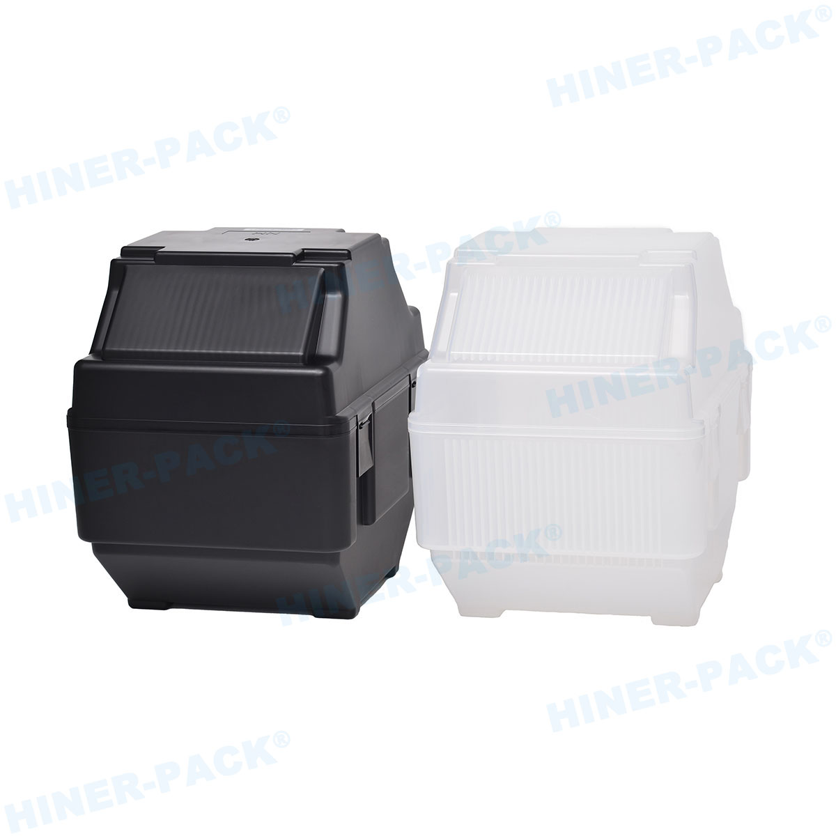
The design of a 2 inch wafer carrier is a marvel of engineering, tailored to meet stringent industry standards. Most carriers feature a rigid frame with multiple slots, each precisely spaced to accommodate 2-inch wafers without causing stress or contact that could lead to cracks or contamination. The number of slots can vary, with common configurations holding 25 to 50 wafers, depending on the application. Materials selection is critical; carriers are often made from advanced polymers like polycarbonate or PEEK (polyether ether ketone), which offer excellent chemical resistance and low particulate generation. For high-temperature processes, carriers may be crafted from stainless steel or other metals coated with protective layers to prevent corrosion.
Another key aspect of the 2 inch wafer carrier design is its focus on cleanliness. In semiconductor environments, even microscopic particles can ruin a batch of wafers. Thus, carriers are designed with smooth surfaces and minimal crevices to facilitate easy cleaning. Many models include static-dissipative properties to prevent electrostatic discharge, which can damage sensitive circuits. Additionally, modern 2 inch wafer carrier designs often incorporate ergonomic handles and stacking features for efficient storage and transport. Some advanced versions are compatible with SMIF (Standard Mechanical Interface) systems, allowing for seamless integration into automated production lines. This attention to detail in design ensures that the 2 inch wafer carrier not only protects wafers but also enhances overall operational efficiency.
Applications in the Semiconductor Industry
The 2 inch wafer carrier finds extensive use across various segments of the semiconductor industry. In research and development labs, it enables safe handling of prototype wafers during experimentation with new materials or processes. For instance, in photolithography, wafers must be moved between exposure and development stages without exposure to contaminants—a task perfectly suited for the 2 inch wafer carrier. Similarly, in etching and deposition processes, the carrier ensures wafers are positioned correctly in equipment, reducing alignment errors and improving yield rates.
In high-volume manufacturing, the 2 inch wafer carrier is integral to assembly lines. It is commonly used in front-end processes like wafer probing and testing, where individual dies are evaluated for functionality. The carrier's ability to maintain wafer orientation simplifies automation, leading to faster cycle times. Moreover, in back-end operations such as packaging and dicing, the 2 inch wafer carrier protects wafers from mechanical stress. Beyond traditional semiconductors, these carriers are also employed in emerging fields like MEMS (Micro-Electro-Mechanical Systems) and photovoltaics, where precision handling is equally critical. The versatility of the 2 inch wafer carrier makes it a staple in any facility dealing with small-diameter wafers, underscoring its importance in driving innovation and productivity.
Advantages of Using 2-Inch Wafer Carriers
Utilizing a 2 inch wafer carrier offers numerous advantages that directly impact manufacturing outcomes. First and foremost, it provides superior protection against physical damage and contamination. Wafers are extremely fragile, and even slight impacts can cause cracks or breaks. The carrier's snug fit and robust construction mitigate these risks, leading to lower scrap rates and cost savings. Additionally, the 2 inch wafer carrier enhances workflow efficiency by standardizing wafer handling. This consistency reduces human error and training time, as operators can rely on the carrier's design for safe transport.
Another significant benefit is compatibility with automation. Many 2 inch wafer carrier models are designed to interface with robotic systems, enabling unattended operation in cleanrooms. This not only boosts throughput but also minimizes human-induced contamination. Furthermore, the reusable nature of these carriers supports sustainability efforts by reducing waste compared to disposable alternatives. From a quality assurance perspective, the 2 inch wafer carrier allows for better traceability, especially when integrated with barcoding or RFID systems. This helps in tracking wafer lots throughout the production cycle, ensuring compliance with industry standards. In summary, the 2 inch wafer carrier is a cost-effective solution that promotes reliability, scalability, and environmental responsibility in semiconductor manufacturing.
How to Choose the Right 2-Inch Wafer Carrier
Selecting the appropriate 2 inch wafer carrier requires careful consideration of several factors to match specific operational needs. Start by assessing the material compatibility with your processes. For instance, if your environment involves aggressive chemicals, opt for carriers made from chemically resistant polymers like PTFE or metals with protective coatings. The slot pitch and capacity of the 2 inch wafer carrier are also crucial; ensure they align with your wafer thickness and storage requirements to avoid overcrowding or wasted space.
Another key criterion is the level of automation in your facility. If you use robotic handlers, choose a 2 inch wafer carrier with standardized dimensions and features like alignment notches for seamless integration. Static control is another aspect—look for carriers with ESD (electrostatic discharge) protection to safeguard sensitive wafers. Additionally, consider the carrier's cleanability; models with smooth, non-porous surfaces are easier to decontaminate in cleanroom settings. Finally, evaluate the supplier's reputation and support services. A reliable 2 inch wafer carrier provider should offer customization options and adherence to industry certifications like SEMI standards. By taking these factors into account, you can invest in a carrier that maximizes efficiency and minimizes risks in your operations.
Maintenance and Best Practices for 2-Inch Wafer Carriers
Proper maintenance of a 2 inch wafer carrier is essential to prolong its lifespan and ensure consistent performance. Regular cleaning is the cornerstone of upkeep; carriers should be cleaned in a controlled environment using approved solvents like isopropyl alcohol or deionized water. Ultrasonic cleaners can be effective for removing stubborn contaminants without damaging the carrier. After cleaning, inspect the 2 inch wafer carrier for signs of wear, such as cracks or deformities, which could compromise wafer safety. If any damage is detected, replace the carrier promptly to avoid production delays.
Storage practices also play a vital role. Store the 2 inch wafer carrier in a clean, dry area away from direct sunlight and extreme temperatures to prevent material degradation. When handling, always use gloves and follow cleanroom protocols to minimize contamination. For carriers used in high-throughput settings, establish a routine maintenance schedule—for example, monthly inspections and cleanings—to catch issues early. Additionally, train personnel on proper usage techniques, such as avoiding overloading slots and handling carriers with care during transport. By adhering to these best practices, you can maintain the integrity of your 2 inch wafer carrier and support a reliable manufacturing process.
In conclusion, the 2 inch wafer carrier is a fundamental component in semiconductor manufacturing, offering protection, efficiency, and compatibility with modern automation. From its precise design to its diverse applications, this tool enables the high standards required in electronics production. By understanding its features and implementing proper maintenance, businesses can achieve better yields and reduce costs. As technology evolves, the 2 inch wafer carrier will continue to adapt, solidifying its role in the industry.
Frequently Asked Questions
Q1: What is the primary purpose of a 2-inch wafer carrier?
A1: The primary purpose of a 2 inch wafer carrier is to safely hold, protect, and transport 2-inch silicon wafers during semiconductor manufacturing processes. It prevents physical damage, contamination, and electrostatic discharge, ensuring wafers remain intact and clean from production stages like etching to inspection.
Q2: What materials are commonly used in manufacturing 2-inch wafer carriers?
A2: Common materials for 2 inch wafer carrier production include high-purity polymers such as polycarbonate and PEEK, which offer chemical resistance and low particulate generation. For high-temperature applications, stainless steel or coated metals are often used to withstand harsh environments without corroding.
Q3: How do I clean a 2-inch wafer carrier properly?
A3: To clean a 2 inch wafer carrier, use a cleanroom-approved solvent like isopropyl alcohol or deionized water, and consider ultrasonic cleaning for thorough decontamination. Always dry the carrier completely before reuse and inspect it for any damage to maintain optimal performance and cleanliness.
Q4: Can a 2-inch wafer carrier be used for wafers of other sizes?
A4: No, a 2 inch wafer carrier is specifically designed for 2-inch wafers and should not be used for other sizes. Using it for larger or smaller wafers can lead to improper fit, increased risk of damage, and contamination, so it's essential to match the carrier to the wafer diameter.
Q5: What features should I look for when selecting a 2-inch wafer carrier for automated systems?
A5: When choosing a 2 inch wafer carrier for automated systems, look for features like standardized dimensions (e.g., SEMI compliance), alignment notches, RFID compatibility, and static-dissipative properties. These ensure seamless integration with robotics, reduce handling errors, and enhance traceability in high-volume production environments.