In the highly precise world of semiconductor manufacturing, every component plays a vital role in ensuring efficiency, yield, and cost-effectiveness. One such component that often goes unnoticed but is crucial for wafer protection and handling is the wafer clamshell. This specialized container is designed to safeguard delicate semiconductor wafers from contaminants, physical damage, and environmental factors during storage, transport, and processing. As semiconductor nodes shrink to nanometer scales, the demand for reliable wafer clamshell solutions has surged, making it essential for professionals to understand their applications, selection criteria, and technological advancements. This article delves into the key aspects of wafer clamshell systems, providing insights to help you make informed decisions in your semiconductor operations.
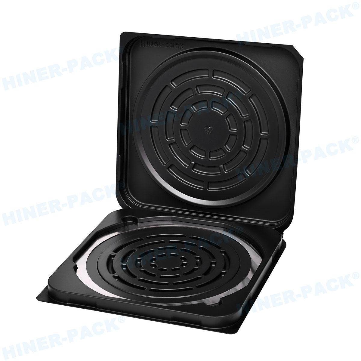
What Is a Wafer Clamshell?
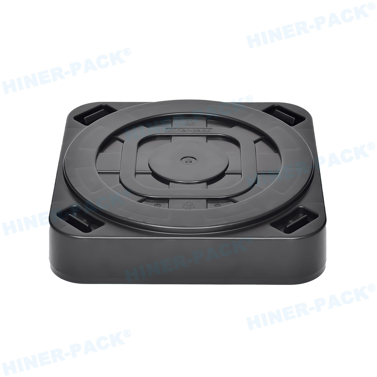
A wafer clamshell is a protective enclosure typically made from high-purity materials like polymers or composites, engineered to hold semiconductor wafers securely. Its name derives from its clamshell-like design, which features two hinged halves that open and close to allow easy access to wafers while maintaining a sealed environment. This design minimizes exposure to particles, moisture, and static electricity, which are critical concerns in cleanroom settings. The wafer clamshell is often used in conjunction with front-opening unified pods (FOUPs) or other wafer carriers, providing an additional layer of security for high-value wafers during logistics and manufacturing stages. In essence, it acts as a first line of defense against defects that could compromise integrated circuit performance.
The evolution of the wafer clamshell has been driven by the semiconductor industry's push toward smaller feature sizes and higher wafer diameters, such as 300mm and beyond. Modern versions incorporate features like RFID tagging for tracking, ergonomic handles for manual handling, and compatibility with automated systems. Understanding the basic structure and function of a wafer clamshell is the first step toward appreciating its role in enhancing overall process reliability.
Key Applications of Wafer Clamshell in Semiconductor Manufacturing
The wafer clamshell finds its place across various stages of semiconductor production, from fabrication to testing and shipping. One primary application is in wafer transport between facilities. As wafers move from foundries to assembly sites, the wafer clamshell ensures they remain uncontaminated and undamaged, even under varying environmental conditions. This is particularly important for wafers with advanced nodes, where even minor particles can lead to yield losses.
Another critical use is in temporary storage within cleanrooms. During process queues, wafers may need to be held for hours or days, and the wafer clamshell provides a stable, controlled environment that prevents oxidation and electrostatic discharge (ESD). Additionally, in metrology and inspection processes, the wafer clamshell allows for safe loading and unloading of wafers into measurement tools, reducing handling errors. For instance, in lithography steps, where precision is paramount, using a robust wafer clamshell can minimize misalignment issues caused by external disturbances.
Moreover, the wafer clamshell is integral to back-end operations like dicing and packaging. It protects wafers during transitions between equipment, such as from grinders to bonders, ensuring that micro-cracks or scratches do not occur. As the industry adopts more heterogeneous integration techniques, the role of the wafer clamshell in maintaining wafer integrity becomes even more pronounced, highlighting its versatility in modern semiconductor workflows.
How to Choose the Right Wafer Clamshell: 5 Essential Factors
Selecting an appropriate wafer clamshell requires careful consideration of several factors to match specific operational needs. Here are five critical elements to evaluate:
Material Compatibility and Purity: The material of the wafer clamshell must be non-outgassing and resistant to chemicals used in semiconductor processes, such as acids and solvents. Common materials include high-density polyethylene (HDPE) or polycarbonate blends, which offer low particulate generation. Ensure the material meets industry standards like SEMI guidelines to avoid contamination that could affect wafer surfaces.
Design and Ergonomics: A well-designed wafer clamshell should feature smooth, rounded edges to prevent snagging and easy-open mechanisms for efficient handling. Consider factors like weight, stackability, and compatibility with existing automation systems. For high-volume facilities, opt for clamshells that integrate with robotic arms to reduce manual intervention and improve throughput.
Environmental Protection: Look for wafer clamshell options that provide adequate sealing against moisture, gases, and particulates. Features like gaskets or latch locks can enhance protection, especially in humid or dusty environments. This is crucial for processes involving sensitive materials like copper or low-k dielectrics, where oxidation can lead to failures.
Cost and Lifespan: While initial cost is a factor, prioritize durability and reusability. A higher-priced wafer clamshell made from robust materials might offer better long-term value by reducing replacement frequency and downtime. Calculate the total cost of ownership, including cleaning and maintenance, to make an economical choice.
Regulatory and Standards Compliance: Ensure the wafer clamshell adheres to international standards, such as SEMI S2 for safety or ISO 14644 for cleanroom compatibility. This not only guarantees performance but also facilitates global supply chain integration, which is vital for multinational semiconductor operations.
By addressing these factors, you can select a wafer clamshell that enhances process efficiency while safeguarding your wafer investments.
Cost Considerations for Wafer Clamshell Implementation
When integrating wafer clamshell systems into semiconductor processes, cost analysis goes beyond the purchase price. Initial expenses include the unit cost of the clamshells, which can range from a few dollars to over a hundred dollars per unit, depending on material quality and features. However, operational costs such as cleaning, sterilization, and potential downtime due to clamshell failure must also be accounted for. For example, a low-cost wafer clamshell might require frequent replacements, leading to higher long-term expenditures and increased risk of wafer damage.
Volume discounts and supplier agreements can help mitigate costs, especially for large-scale fabs. Additionally, consider the cost savings from improved yield—using a reliable wafer clamshell can reduce defect rates by 1-2%, which translates to significant financial gains in high-volume production. Leasing or recycling programs for wafer clamshell units are also emerging trends, offering flexibility for companies with fluctuating demands. Ultimately, a balanced approach that weighs upfront investment against lifecycle benefits will ensure optimal resource allocation in your semiconductor budget.
Technological Advancements in Wafer Clamshell Design
The wafer clamshell has evolved significantly, driven by innovations in materials science and automation. Recent advancements include the development of "smart" wafer clamshell systems embedded with sensors that monitor internal conditions like temperature, humidity, and shock levels. These IoT-enabled clamshells provide real-time data to predictive maintenance systems, allowing proactive interventions that minimize wafer loss.
Another trend is the use of advanced composites with anti-static properties, which reduce ESD risks in sensitive processes. Manufacturers are also exploring lightweight, biodegradable materials to align with sustainability goals, without compromising protection. In terms of design, modular wafer clamshell configurations are gaining traction, enabling customization for different wafer sizes and process requirements. For instance, clamshells with adjustable compartments can accommodate varying wafer thicknesses, enhancing versatility in R&D environments.
Furthermore, automation compatibility has been a focus, with new wafer clamshell models featuring standardized interfaces for seamless integration into Industry 4.0 frameworks. These innovations not only improve operational efficiency but also support the semiconductor industry's move toward more agile and resilient supply chains.
The wafer clamshell may seem like a minor accessory in the grand scheme of semiconductor manufacturing, but its impact on wafer integrity, yield, and overall process efficiency cannot be overstated. By understanding its applications, selection criteria, costs, and technological trends, professionals can leverage this tool to enhance their operations. As the industry continues to advance, the wafer clamshell will undoubtedly play a pivotal role in enabling next-generation semiconductor technologies. Whether you're involved in fab management, logistics, or process engineering, investing time in evaluating wafer clamshell options will pay dividends in reliability and performance.
Frequently Asked Questions (FAQ)
Q1: What is the primary purpose of a wafer clamshell in semiconductor manufacturing?
A1: The primary purpose of a wafer clamshell is to protect semiconductor wafers from physical damage, contamination, and environmental factors during storage, transport, and handling. It acts as a secure enclosure that maintains wafer integrity in cleanroom and logistics environments, reducing the risk of defects and yield loss.
Q2: How does a wafer clamshell differ from standard wafer carriers?
A2: While standard wafer carriers like FOUPs are designed for automated processing within tools, a wafer clamshell often serves as an additional protective layer during external transport or temporary storage. It typically features a clamshell-style opening for easy access and enhanced sealing, whereas carriers focus on integration with specific equipment.
Q3: What materials are commonly used in wafer clamshell production?
A3: Common materials for wafer clamshell include high-purity plastics such as polycarbonate, HDPE, or PEEK, chosen for their low particulate generation, chemical resistance, and durability. These materials comply with industry standards to ensure they do not introduce contaminants into sensitive semiconductor processes.
Q4: Can wafer clamshells be reused, and how should they be maintained?
A4: Yes, many wafer clamshell units are reusable. Maintenance typically involves regular cleaning with deionized water or specialized solvents to remove residues, followed by inspections for wear and tear. Proper storage in clean environments and adherence to manufacturer guidelines can extend their lifespan and ensure consistent performance.
Q5: What are the cost implications of choosing a low-quality wafer clamshell?
A5: Opting for a low-quality wafer clamshell can lead to higher long-term costs due to increased failure rates, frequent replacements, and potential wafer damage. This may result in production downtime, yield losses, and additional expenses for cleaning and disposal, outweighing any initial savings from a cheaper purchase price.


