
In the fast-paced semiconductor industry, the safe and efficient transport of silicon wafers is critical to maintaining product integrity and minimizing costly disruptions. At the heart of this process lies the wafer shipping carrier, a specialized container designed to protect delicate wafers from physical damage, contamination, and environmental hazards during transit. As technology advances and wafer sizes increase, the demand for reliable shipping solutions has never been higher. This article delves into the essential aspects of wafer shipping carrier systems, exploring custom solutions, the importance of 300mm variants, cleaning services, and manufacturer selection. We will also address common problems faced in wafer shipping and provide practical insights to optimize your logistics. Whether you are a fab manager, logistics coordinator, or industry newcomer, understanding these elements can enhance your operational efficiency and safeguard your investments.
Understanding the Wafer Shipping Carrier
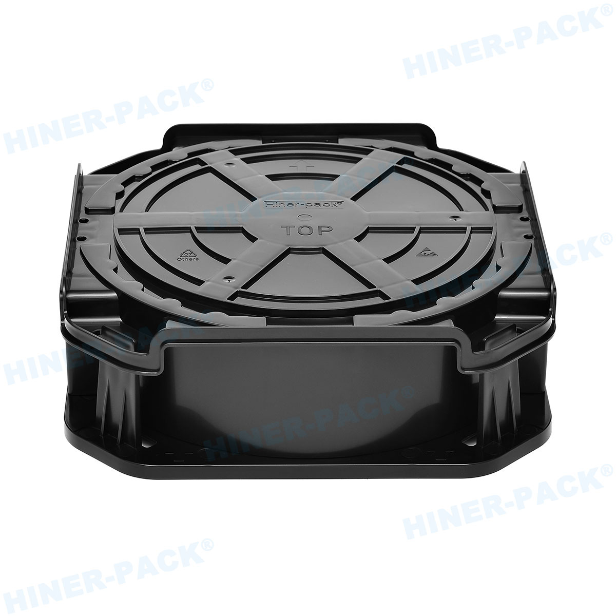
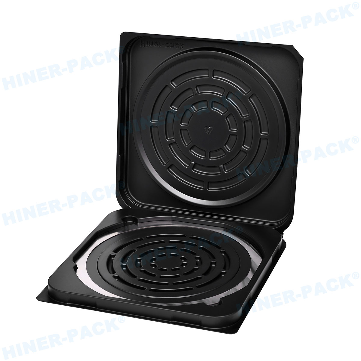
A wafer shipping carrier is a precision-engineered container used to transport silicon wafers between manufacturing facilities, testing sites, and end-users. These carriers are typically made from materials like polycarbonate or advanced polymers that offer static dissipation, minimal particulate generation, and robust structural integrity. The primary function of a wafer shipping carrier is to isolate wafers from external threats such as moisture, dust, and mechanical shocks, which could compromise the sensitive microstructures on the wafer surface. In modern semiconductor operations, the wafer shipping carrier is not just a box but a integral part of the supply chain, ensuring that wafers arrive in pristine condition for further processing or assembly.
The design of a wafer shipping carrier varies based on wafer size, with common configurations for 200mm, 300mm, and emerging 450mm wafers. Each carrier includes features like secure locking mechanisms, cushioned slots, and environmental seals to maintain a controlled internal atmosphere. For instance, in high-volume production, a wafer shipping carrier might incorporate RFID tracking for real-time monitoring. The evolution of these carriers has been driven by industry standards such as SEMI guidelines, which specify dimensions, materials, and performance criteria. As wafers become thinner and more fragile, the role of the wafer shipping carrier in preventing warpage and breakage becomes increasingly vital. Moreover, with the rise of global supply chains, the wafer shipping carrier must withstand varying transportation conditions, from air freight to ground shipping, without compromising protection.
In practice, selecting the right wafer shipping carrier involves considering factors like wafer type, shipping distance, and regulatory requirements. For example, carriers used in the automotive or aerospace sectors may need to meet stricter cleanliness standards due to the critical nature of their applications. By understanding the fundamentals of the wafer shipping carrier, businesses can make informed decisions that reduce risks and improve overall logistics performance.
Custom Wafer Shipping Solutions for Specific Needs
In today's diverse semiconductor landscape, one-size-fits-all approaches often fall short. This is where a custom wafer shipping solution comes into play, offering tailored designs to meet unique operational requirements. A custom wafer shipping solution involves collaborating with experts to develop carriers that address specific challenges, such as handling ultra-thin wafers, integrating with automated systems, or complying with international shipping regulations. For instance, a company dealing with sensitive photonic devices might need a custom wafer shipping solution with enhanced anti-vibration properties and specialized padding to prevent micro-cracks.
The benefits of a custom wafer shipping solution extend beyond mere protection. It can optimize space utilization in shipping containers, reduce material costs, and streamline handling processes. Many wafer shipping carrier manufacturer offer design services that include prototyping and testing to ensure the solution meets performance benchmarks. A well-executed custom wafer shipping solution might feature modular components, allowing for easy adaptation to different wafer sizes or quantities. This flexibility is crucial in industries like medical devices or research, where batch sizes vary widely.
Moreover, a custom wafer shipping solution can incorporate sustainability elements, such as reusable materials or eco-friendly packaging, aligning with corporate environmental goals. For example, some manufacturers provide carriers made from recyclable polymers that maintain high cleanliness levels. When implementing a custom wafer shipping solution, it's essential to conduct a thorough needs assessment, considering factors like transit time, storage conditions, and compatibility with existing equipment. By investing in a custom wafer shipping solution, companies can achieve higher yield rates, lower rejection costs, and enhanced supply chain resilience. In essence, a custom wafer shipping solution transforms the wafer shipping carrier from a passive container into an active tool for operational excellence.
The Critical Role of the 300mm Wafer Shipper
As the semiconductor industry shifts toward larger wafer sizes to boost productivity and reduce per-unit costs, the 300mm wafer shipper has become a cornerstone of modern manufacturing. The 300mm wafer shipper is specifically designed to accommodate 300mm diameter wafers, which are prevalent in advanced nodes for applications like processors, memory chips, and IoT devices. Unlike smaller counterparts, the 300mm wafer shipper must handle greater weight and surface area, requiring robust construction to prevent sagging or damage during transit. These carriers often feature reinforced walls, precision-molded slots, and advanced latching systems to secure wafers in place.
The importance of the 300mm wafer shipper lies in its ability to maintain wafer integrity across complex supply chains. With 300mm wafers representing a significant portion of global production, any failure in shipping can lead to substantial financial losses. Therefore, the 300mm wafer shipper is engineered to meet stringent SEMI standards, including guidelines for dimensional stability, electrostatic discharge (ESD) protection, and contamination control. Many 300mm wafer shipper models include environmental monitors that track temperature, humidity, and shock events, providing data logs for quality assurance.
In addition, the 300mm wafer shipper is often integrated with factory automation systems, enabling seamless transfer between tools without manual intervention. This compatibility reduces handling time and minimizes human error. However, the larger size of the 300mm wafer shipper also presents challenges, such as higher shipping costs and storage requirements. To address this, manufacturers are developing lightweight yet durable designs that optimize logistics efficiency. For businesses relying on 300mm technology, selecting a high-quality 300mm wafer shipper is non-negotiable for maintaining throughput and product quality. As the industry explores even larger wafers, the lessons learned from the 300mm wafer shipper will inform future innovations in wafer transport.
Ensuring Cleanliness with Wafer Carrier Cleaning Service
Contamination is a perennial threat in semiconductor manufacturing, and even minute particles can ruin entire wafer batches. This makes a professional wafer carrier cleaning service an indispensable part of the logistics cycle. A wafer carrier cleaning service involves the systematic cleaning, inspection, and recertification of wafer shipping carrier units to ensure they meet purity standards before reuse. These services use specialized equipment, such as ultrasonic cleaners, deionized water rinses, and particle counters, to remove residues, dust, and ionic contaminants that accumulate during transit or storage.
The value of a wafer carrier cleaning service extends beyond basic hygiene. Regular cleaning prolongs the lifespan of carriers, reduces the risk of cross-contamination between batches, and helps comply with industry regulations like ISO 14644 for cleanrooms. Many wafer shipping carrier manufacturer offer integrated wafer carrier cleaning service programs, providing convenience and consistency. For example, a typical wafer carrier cleaning service might include steps like disassembly, chemical treatment, drying, and functional testing to verify that seals and locks remain effective.
In high-volume fabs, outsourcing to a dedicated wafer carrier cleaning service can be more cost-effective than maintaining in-house facilities, as it frees up resources and ensures expert handling. Moreover, a reliable wafer carrier cleaning service often provides documentation certifying cleanliness levels, which is crucial for audit trails and quality control. Common issues addressed by a wafer carrier cleaning service include particulate buildup, static charge accumulation, and biological growth in humid environments. By partnering with a trusted wafer carrier cleaning service, companies can minimize yield loss, enhance product reliability, and maintain a smooth production flow. Ultimately, integrating a wafer carrier cleaning service into your logistics strategy is a proactive step toward safeguarding your wafer investments.
Selecting a Reliable Wafer Shipping Carrier Manufacturer
Choosing the right wafer shipping carrier manufacturer is a critical decision that impacts product safety, cost efficiency, and supply chain reliability. A reputable wafer shipping carrier manufacturer should offer a comprehensive portfolio, including standard and custom designs, and demonstrate a deep understanding of semiconductor industry needs. Key factors to consider when evaluating a wafer shipping carrier manufacturer include their material quality, manufacturing processes, compliance with standards, and after-sales support. For instance, a top-tier wafer shipping carrier manufacturer will use certified materials that resist outgassing and ESD, and employ precision molding techniques to ensure consistent product dimensions.
Experience and innovation are hallmarks of a leading wafer shipping carrier manufacturer. Look for manufacturers with a track record of serving major semiconductor companies and those who invest in R&D to address emerging challenges, such as the demand for greener materials or smarter carriers with IoT capabilities. A good wafer shipping carrier manufacturer will also provide testing data and case studies to validate their products' performance under real-world conditions. Additionally, consider the manufacturer's global presence and logistics network, as this can affect lead times and service accessibility.
Another aspect is the ability to offer value-added services, such as the wafer carrier cleaning service or consultation for a custom wafer shipping solution. A collaborative wafer shipping carrier manufacturer can help you optimize your entire shipping process, from design to maintenance. It's also wise to assess their quality control measures, such as ISO 9001 certification, which ensures consistent production standards. By conducting due diligence and possibly requesting samples, you can select a wafer shipping carrier manufacturer that aligns with your operational goals and risk tolerance. In the long run, a strong partnership with a reliable wafer shipping carrier manufacturer can lead to improved efficiency, lower total cost of ownership, and enhanced product protection.
Common Challenges in Wafer Shipping and How to Overcome Them
Despite advancements in carrier technology, several common problems persist in wafer shipping. Understanding these issues and their solutions can help mitigate risks and improve outcomes. One frequent challenge is contamination, which can originate from inadequate cleaning, poor handling, or environmental exposure. To combat this, implement a rigorous wafer carrier cleaning service routine and use carriers with advanced sealing features. Additionally, train staff on proper handling protocols and monitor cleanroom conditions during loading and unloading.
Another issue is physical damage, such as wafer chipping or breakage due to shock or vibration during transit. This is particularly relevant for larger wafers like those in a 300mm wafer shipper. Solutions include using carriers with cushioned slots, shock-absorbing materials, and real-time monitoring devices that alert to excessive impacts. Working with a wafer shipping carrier manufacturer to develop a custom wafer shipping solution with enhanced protection can also reduce this risk. For example, incorporating foam inserts or suspension systems can dissipate forces more effectively.
Electrostatic discharge (ESD) is a hidden threat that can damage sensitive circuits. Ensure that your wafer shipping carrier is made from ESD-safe materials and regularly tested for static dissipation. Humidity control is another concern, as moisture can lead to corrosion or adhesion problems. Using carriers with desiccant packs or humidity indicators, and selecting a custom wafer shipping solution with climate control options, can help maintain optimal conditions.
Logistical delays and miscommunication can also disrupt wafer shipments. To address this, establish clear tracking systems and collaborate with reliable logistics partners. Common problems like carrier misalignment in automated systems can be avoided by adhering to SEMI standards and conducting regular maintenance. Finally, cost pressures often lead to compromises in carrier quality, but this can backfire with higher failure rates. Instead, focus on total cost of ownership by investing in durable carriers and preventive services like the wafer carrier cleaning service. By proactively addressing these challenges, companies can enhance the reliability of their wafer shipping processes and protect valuable semiconductor assets.
The wafer shipping carrier is more than just a container; it is a vital component in the semiconductor supply chain that ensures the safe delivery of high-value wafers. From adopting a custom wafer shipping solution to leveraging the capabilities of a 300mm wafer shipper, businesses can tailor their approaches to meet specific needs. Incorporating a professional wafer carrier cleaning service maintains cleanliness and prolongs carrier life, while selecting a trustworthy wafer shipping carrier manufacturer lays the foundation for long-term success. By understanding and addressing common shipping problems, companies can minimize risks and optimize their operations. As the industry evolves, continuous innovation in wafer shipping carrier technology will play a key role in supporting the growth of advanced electronics. Embrace these insights to strengthen your logistics strategy and achieve greater efficiency in wafer transport.


