
In the fast-paced world of semiconductor manufacturing, precision and reliability are paramount. One critical component that often goes unnoticed but plays a vital role in ensuring the integrity of silicon wafers is the 100mm wafer carrier. This essential tool is designed to protect and transport wafers during various stages of production, from fabrication to testing. As the demand for smaller, more efficient electronic devices grows, the importance of high-quality wafer carriers cannot be overstated. In this article, we will explore the intricacies of the 100mm wafer carrier, including its manufacturing processes, the role of a trusted wafer carrier manufacturer, comparisons with 4 inch wafer carrier options, applications in Semiconductor wafer carrier systems, and the advantages of opting for a Custom 100mm wafer carrier. Additionally, we will address common questions and challenges faced by industry professionals, providing a comprehensive resource for those involved in semiconductor handling. Whether you are a seasoned engineer or a newcomer to the field, understanding these aspects can enhance your operational efficiency and product quality.
What Is a 100mm Wafer Carrier?
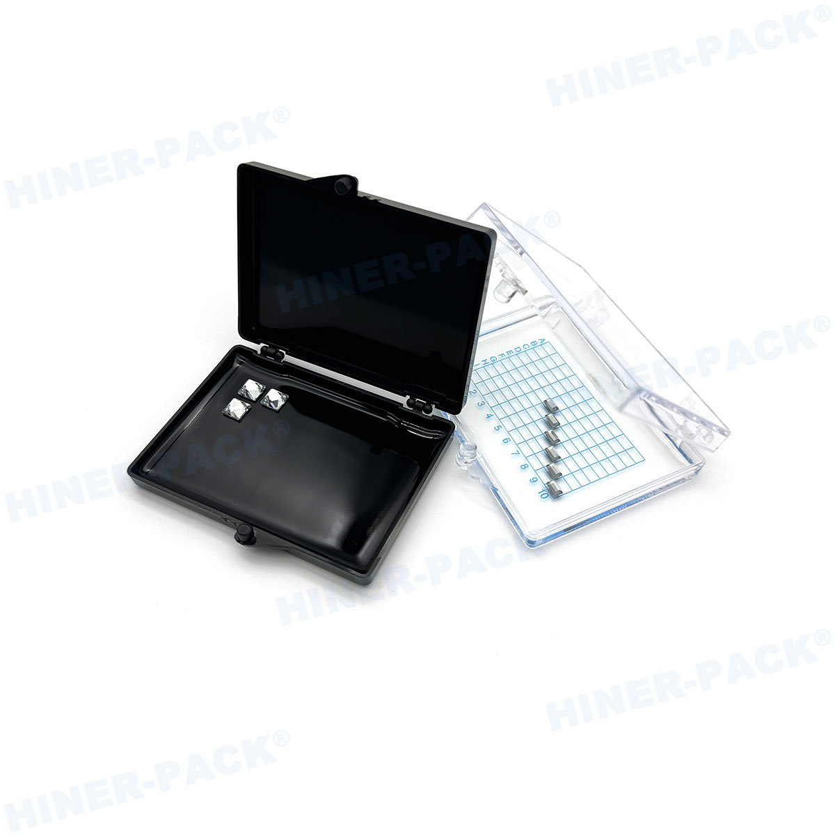
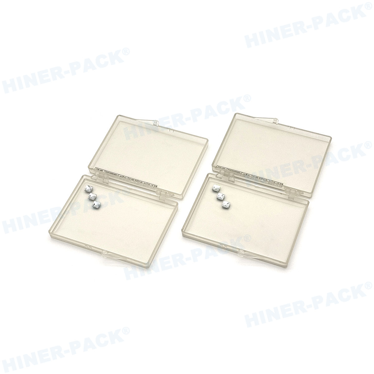
A 100mm wafer carrier is a specialized container used to hold and protect 100mm diameter silicon wafers during storage, transport, and processing in semiconductor facilities. These carriers are typically made from materials like polycarbonate, polypropylene, or other high-purity plastics to minimize contamination and static discharge. The design includes precise slots or grooves to securely hold each wafer, preventing contact and damage that could lead to yield losses. Given that 100mm wafers are commonly used in research, development, and small-scale production, the 100mm wafer carrier must meet stringent standards for cleanliness and durability. In many ways, it serves as the first line of defense against environmental factors such as dust, moisture, and physical shocks. As semiconductor technology advances, the need for robust 100mm wafer carrier solutions becomes even more critical, especially when integrating with automated systems. This is where partnering with an experienced wafer carrier manufacturer can make a significant difference, ensuring that the carriers are tailored to specific operational requirements.
The Role of a Professional Wafer Carrier Manufacturer
Choosing the right wafer carrier manufacturer is crucial for maintaining the integrity of semiconductor processes. A reputable manufacturer not only produces carriers that meet industry standards but also provides customization options to address unique challenges. For instance, a manufacturer like Hiner-pack specializes in developing 100mm wafer carrier units that are compatible with various equipment and environments. They employ advanced injection molding techniques and rigorous testing protocols to ensure each carrier offers low particulate generation, high thermal stability, and anti-static properties. Moreover, a reliable wafer carrier manufacturer often conducts research and development to innovate new designs, such as carriers with improved ergonomics or enhanced compatibility with robotics. This proactive approach helps clients reduce downtime and increase throughput. When selecting a manufacturer, it's important to consider factors like material quality, certifications (e.g., ISO standards), and customer support. By collaborating with a trusted wafer carrier manufacturer, companies can mitigate risks associated with wafer damage and contamination, ultimately leading to higher yields and cost savings.
4 Inch Wafer Carrier vs. 100mm: Understanding the Equivalence
In the semiconductor industry, the terms 4 inch wafer carrier and 100mm wafer carrier are often used interchangeably, as 100mm is approximately equal to 4 inches. However, subtle differences in design and application can arise based on regional standards or specific customer preferences. A 4 inch wafer carrier typically refers to carriers designed for wafers with a diameter of 4 inches (about 101.6mm), but in practice, many manufacturers, including Hiner-pack, produce carriers that accommodate both 100mm and 4-inch wafers due to their close dimensions. The key consideration here is compatibility with existing equipment; for example, some older fabrication tools might be calibrated for exact 4-inch wafers, while newer systems are optimized for metric measurements. When sourcing a 100mm wafer carrier, it's essential to verify the specifications to ensure a proper fit. This highlights the importance of working with a knowledgeable wafer carrier manufacturer who can provide guidance on the best options for your needs. Additionally, customizations in a Custom 100mm wafer carrier can bridge any gaps, offering tailored solutions that align with both metric and imperial systems.
Applications of Semiconductor Wafer Carriers
Semiconductor wafer carrier systems are integral to the entire lifecycle of wafer production, from crystal growth to packaging. The 100mm wafer carrier, in particular, finds applications in various settings, including academic research, pilot lines, and specialized manufacturing processes. For example, in cleanrooms, these carriers help maintain wafer cleanliness by minimizing exposure to contaminants. They are also used in transport between different departments, such as from lithography to etching, where precise alignment is necessary to avoid misprocessing. In automated environments, a Semiconductor wafer carrier must interface seamlessly with robotic arms and conveyor systems, which requires designs that include features like RFID tags or barcodes for tracking. The versatility of the 100mm wafer carrier makes it suitable for handling not only silicon wafers but also other substrates like gallium arsenide in optoelectronics. As technology evolves, the demand for specialized Semiconductor wafer carrier solutions continues to grow, driving innovations in materials and designs. This is where a Custom 100mm wafer carrier can offer significant advantages, allowing for modifications that cater to specific application requirements, such as high-temperature resistance or anti-vibration properties.
Benefits of Choosing a Custom 100mm Wafer Carrier
Opting for a Custom 100mm wafer carrier can provide numerous benefits over off-the-shelf solutions, especially in highly specialized semiconductor operations. Customization allows for adjustments in material composition, slot count, and structural features to match unique process needs. For instance, a Custom 100mm wafer carrier might include additional padding for fragile wafers, integrated sensors for environmental monitoring, or modified dimensions to fit non-standard equipment. This level of personalization is often facilitated by a collaborative wafer carrier manufacturer like Hiner-pack, which works closely with clients to design carriers that optimize workflow efficiency. Moreover, a Custom 100mm wafer carrier can enhance scalability; as production volumes change, carriers can be adapted to handle varying batch sizes without compromising on protection. Cost-effectiveness is another advantage, as tailored carriers reduce the risk of wafer loss due to incompatibility issues. In industries where precision is non-negotiable, investing in a Custom 100mm wafer carrier can lead to long-term savings and improved product quality. It's worth noting that customization also extends to aesthetics and branding, with options for color coding or logo imprinting to aid in inventory management.
Common Questions About 100mm Wafer Carriers
When working with 100mm wafer carrier systems, professionals often encounter several common questions and challenges. Addressing these can help in making informed decisions and avoiding potential pitfalls.
How do I clean and maintain a 100mm wafer carrier?
Proper maintenance is essential to prevent contamination. Most 100mm wafer carrier units can be cleaned using deionized water and isopropyl alcohol, followed by drying in a controlled environment. It's recommended to follow the manufacturer's guidelines, such as those provided by Hiner-pack, to avoid material degradation. Regular inspections for cracks or wear are also advised.
What materials are best for a Semiconductor wafer carrier?
Materials like polycarbonate and PEEK (polyether ether ketone) are popular due to their low particulate shedding and high durability. The choice depends on the application; for high-temperature processes, a Custom 100mm wafer carrier made from advanced thermoplastics might be necessary.
Can a 4 inch wafer carrier be used interchangeably with a 100mm version?
While they are similar, it's crucial to check dimensional tolerances. In most cases, a 100mm wafer carrier will fit 4-inch wafers, but slight variations could cause issues. Consulting with a wafer carrier manufacturer can ensure compatibility.
What are the common causes of wafer damage in carriers?
Damage often results from improper handling, static electricity, or carrier misalignment. Using anti-static materials and ensuring a snug fit in a Semiconductor wafer carrier can mitigate these risks. Custom designs, such as those from Hiner-pack, often include features to address these concerns.
How does customization affect lead times and costs?
Ordering a Custom 100mm wafer carrier may involve longer lead times and higher initial costs due to design and tooling requirements. However, the long-term benefits in terms of reduced waste and improved efficiency often justify the investment.
Are there industry standards for 100mm wafer carriers?
Yes, organizations like SEMI (Semiconductor Equipment and Materials International) set standards for dimensions and materials. Reputable manufacturers adhere to these to ensure interoperability and safety.
By understanding these aspects, users can better navigate the selection and use of 100mm wafer carrier products, leading to more reliable semiconductor manufacturing processes.
Spotlight on Hiner-pack: Innovative Solutions for Wafer Carriers
Hiner-pack has established itself as a leading wafer carrier manufacturer, known for its high-quality 100mm wafer carrier solutions. With a focus on innovation and customer satisfaction, Hiner-pack offers a range of products that include standard and Custom 100mm wafer carrier options. Their carriers are designed to meet the rigorous demands of the semiconductor industry, featuring attributes such as high chemical resistance, low outgassing, and compatibility with automation systems. For instance, their Semiconductor wafer carrier line incorporates advanced polymers that extend product lifespan while maintaining purity levels. Hiner-pack also emphasizes sustainability, using recyclable materials wherever possible. By leveraging state-of-the-art manufacturing techniques, they ensure that each 100mm wafer carrier is precision-engineered for optimal performance. Clients who have partnered with Hiner-pack report significant improvements in handling efficiency and a reduction in wafer-related defects. This brand's commitment to excellence makes it a go-to choice for those seeking reliable 4 inch wafer carrier and 100mm wafer carrier solutions in a competitive market.
In conclusion, the 100mm wafer carrier is a fundamental component in semiconductor manufacturing, with its effectiveness heavily reliant on the expertise of the wafer carrier manufacturer. Understanding the nuances between a 4 inch wafer carrier and its metric counterpart, along with the applications of a Semiconductor wafer carrier, can drive better decision-making. Opting for a Custom 100mm wafer carrier from a trusted provider like Hiner-pack can further enhance operational efficiency and product quality. By addressing common questions and staying informed about industry trends, professionals can ensure that their wafer handling processes remain at the forefront of technology. As the semiconductor landscape continues to evolve, the role of the 100mm wafer carrier will only grow in importance, making it essential to invest in high-quality, tailored solutions.


