
In the fast-paced world of semiconductor manufacturing, precision and reliability are paramount. One critical component that often goes unnoticed but plays a vital role in ensuring the integrity of silicon wafers is the wafer carrier. Specifically, the 150mm wafer carrier has become a staple in many fabrication facilities due to its balance of size, capacity, and efficiency. This article delves into the intricacies of 150mm wafer carriers, exploring their design, applications, and the manufacturers behind them. We'll also compare them with other sizes like the 4 inch wafer carrier and discuss custom solutions, including the custom 100mm wafer carrier. Additionally, we'll address common problems faced by users and how to mitigate them. Whether you're a seasoned engineer or new to the industry, this comprehensive overview will provide valuable insights into semiconductor wafer carrier technology, with a special focus on the brand Hiner-pack.
What is a 150mm Wafer Carrier?
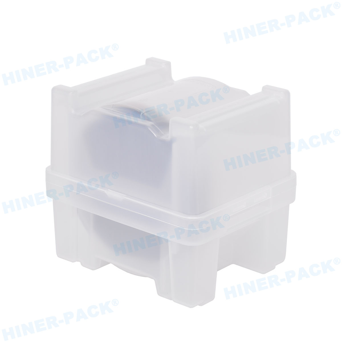
A 150mm wafer carrier is a specialized container designed to hold and transport silicon wafers with a diameter of 150 millimeters (approximately 6 inches) during various stages of semiconductor manufacturing. These carriers are engineered to protect wafers from contaminants, physical damage, and electrostatic discharge, which can compromise the quality of the final product. Made from materials like polycarbonate, polyetheretherketone (PEEK), or other high-purity plastics, a 150mm wafer carrier typically features slots that securely hold wafers in place, allowing for safe handling in cleanroom environments. The design often includes features for automation compatibility, such as robotic handling notches, which streamline processes in high-volume production lines. As semiconductor devices continue to shrink in size and increase in complexity, the role of a reliable 150mm wafer carrier becomes even more critical. It ensures that wafers move seamlessly through etching, deposition, and inspection phases, ultimately contributing to higher yields and reduced downtime. In essence, this carrier is a unsung hero in the semiconductor ecosystem, enabling the precision required for modern electronics.
The Role of a Wafer Carrier Manufacturer
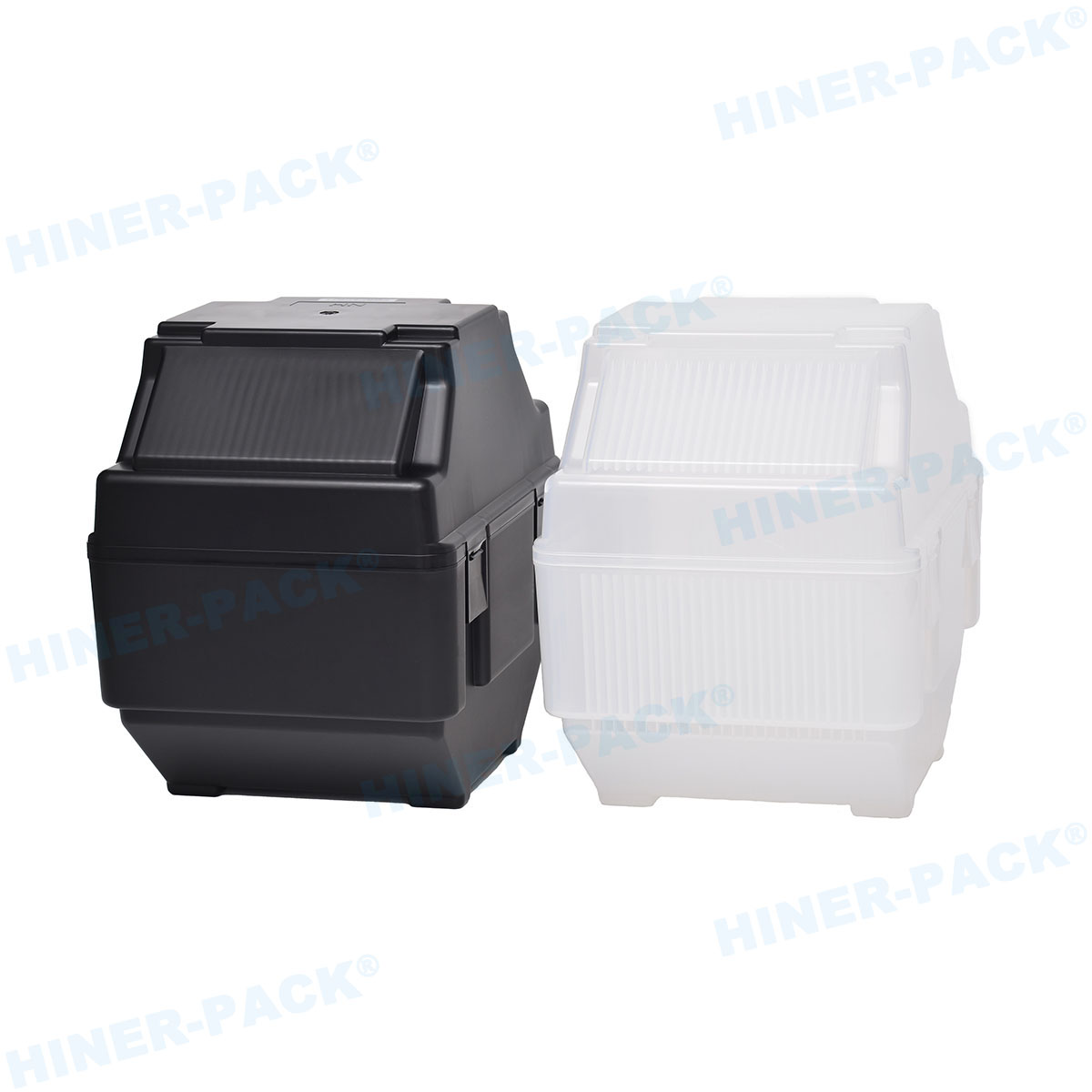
A wafer carrier manufacturer is responsible for producing these essential components to meet the stringent standards of the semiconductor industry. Companies like Hiner-pack specialize in designing and manufacturing wafer carriers that adhere to international cleanliness and durability specifications. These manufacturers employ advanced injection molding techniques and rigorous testing protocols to ensure each carrier meets exact tolerances. For instance, a wafer carrier manufacturer must consider factors like thermal stability, chemical resistance, and particulate generation to prevent contamination. Hiner-pack, in particular, has built a reputation for innovation, offering customized solutions that cater to specific client needs. They work closely with fab operators to develop carriers that integrate with existing equipment, whether for 150mm wafer carriers or smaller variants like the 4 inch wafer carrier. By leveraging materials science and engineering expertise, a wafer carrier manufacturer like Hiner-pack helps drive efficiency in semiconductor production, reducing costs and enhancing overall reliability. Their role extends beyond mere production; they provide technical support and lifecycle management, ensuring that carriers remain functional over time. This partnership between manufacturers and end-users is crucial for maintaining the high standards required in today's competitive market.
Comparing 4 Inch Wafer Carrier and 150mm Options
When evaluating wafer carriers, it's important to understand the differences between a 4 inch wafer carrier and a 150mm wafer carrier. The 4 inch wafer carrier, which corresponds to wafers with a diameter of approximately 100mm, is often used in legacy systems or for specific applications like research and development. In contrast, the 150mm wafer carrier is more common in mainstream semiconductor production due to its larger capacity and compatibility with modern automation. One key distinction is the physical size: a 150mm wafer carrier can hold more wafers per unit, which increases throughput in high-volume fabs. However, the 4 inch wafer carrier may offer advantages in terms of flexibility and cost for smaller batches. For example, a custom 100mm wafer carrier might be tailored for niche processes where precision outweighs scale. In terms of material and design, both types share similarities, such as anti-static properties and cleanroom compatibility, but the 150mm variant often incorporates more advanced features for robotic handling. This makes the 150mm wafer carrier a preferred choice for many semiconductor wafer carrier applications, as it aligns with industry trends toward larger wafers and automated systems. Nonetheless, the 4 inch wafer carrier remains relevant in certain contexts, highlighting the need for manufacturers like Hiner-pack to offer a diverse product range.
Semiconductor Wafer Carrier Essentials
A semiconductor wafer carrier is more than just a storage unit; it is a critical component that ensures the safety and integrity of wafers throughout the manufacturing process. These carriers are designed to minimize particulate contamination, which is a major concern in cleanrooms where even microscopic particles can cause defects. Essential features of a semiconductor wafer carrier include static dissipation to prevent electrostatic discharge, which can damage sensitive circuits, and precise slot alignment to avoid wafer warping or breakage. Materials used must withstand harsh chemical environments and temperature fluctuations common in semiconductor fabrication. For instance, a 150mm wafer carrier often uses high-performance polymers that resist degradation from acids and solvents. Additionally, carriers must be compatible with various processing tools, such as chemical mechanical planarization (CMP) systems and metrology equipment. This interoperability is crucial for seamless production flows. As technology advances, the semiconductor wafer carrier is evolving to support thinner wafers and 3D packaging techniques, requiring even greater precision. Manufacturers like Hiner-pack are at the forefront of these innovations, developing carriers that meet the evolving demands of the industry. By understanding these essentials, fab operators can select the right carrier to optimize their processes and reduce yield loss.
Custom 100mm Wafer Carrier Solutions
In some cases, standard wafer carriers may not meet specific operational requirements, leading to the need for a custom 100mm wafer carrier. These tailored solutions are designed to address unique challenges in semiconductor manufacturing, such as unusual wafer thicknesses, specialized handling needs, or integration with proprietary equipment. A custom 100mm wafer carrier can be optimized for factors like weight reduction, enhanced durability, or specific chemical resistance. For example, a fab dealing with high-temperature processes might require a carrier made from advanced composites that can withstand extreme conditions without releasing contaminants. This level of customization is often provided by experienced wafer carrier manufacturers like Hiner-pack, who collaborate with clients to design carriers that fit exact specifications. While a 150mm wafer carrier is common for general use, the custom 100mm variant offers flexibility for applications like MEMS (Micro-Electro-Mechanical Systems) or photonics, where standard sizes may not suffice. These solutions can also include features like RFID tagging for traceability or modified slot designs to prevent wafer slippage. By investing in a custom 100mm wafer carrier, companies can achieve higher efficiency and reduce the risk of process-related failures, ultimately saving time and resources. Hiner-pack's expertise in this area ensures that even the most demanding requirements are met with precision and reliability.
Common Problems with Wafer Carriers and How to Solve Them
Despite their importance, wafer carriers can encounter several common problems that impact semiconductor production. Understanding these issues and their solutions is key to maintaining optimal performance. One frequent problem is particulate contamination, where debris from the carrier itself or external sources adheres to wafers, leading to defects. This can be mitigated by using high-purity materials and regular cleaning protocols. For instance, a 150mm wafer carrier made from low-particulate-generation polymers, like those offered by Hiner-pack, can reduce this risk. Another issue is mechanical wear and tear, such as slot deformation or cracking, which can cause wafer misalignment or breakage. Regular inspection and replacement of carriers, especially in high-throughput environments, are essential. Electrostatic discharge is also a concern, particularly with older carriers that lack proper static-dissipative properties. Upgrading to carriers with built-in ESD protection can prevent damage to sensitive wafers. Additionally, compatibility problems may arise when integrating carriers with new equipment; working with a reliable wafer carrier manufacturer like Hiner-pack ensures that carriers are designed for seamless interoperability. For a custom 100mm wafer carrier, issues might include design flaws that lead to handling difficulties, which can be addressed through prototyping and testing. Lastly, improper storage or handling by personnel can introduce contaminants—training and automated systems can help minimize human error. By proactively addressing these common problems, fab operators can extend the lifespan of their semiconductor wafer carrier investments and maintain high yield rates.
Why Choose Hiner-pack for Your Wafer Carrier Needs
Hiner-pack stands out as a leading wafer carrier manufacturer, offering a comprehensive range of products, including the 150mm wafer carrier, 4 inch wafer carrier, and custom solutions like the custom 100mm wafer carrier. Their commitment to quality and innovation makes them a trusted partner in the semiconductor industry. Hiner-pack utilizes state-of-the-art manufacturing processes and rigorous quality control to ensure that every carrier meets the highest standards for cleanliness and durability. For example, their 150mm wafer carrier designs incorporate features that enhance robotic handling and reduce particulate generation, aligning with the needs of modern fabs. Moreover, Hiner-pack provides extensive customization options, allowing clients to tailor carriers for specific applications, whether it's a semiconductor wafer carrier for advanced nodes or a specialized variant for research. Their technical support team offers ongoing assistance, from initial design to lifecycle management, ensuring that carriers perform reliably over time. By choosing Hiner-pack, companies benefit from reduced downtime, improved yield, and cost savings. As the industry evolves toward larger wafers and more complex processes, Hiner-pack continues to innovate, developing next-generation carriers that address emerging challenges. This dedication to excellence makes them an ideal choice for anyone seeking reliable wafer carrier solutions.
In summary, the 150mm wafer carrier is a cornerstone of semiconductor manufacturing, offering a balance of size, capacity, and efficiency that supports high-volume production. Throughout this article, we've explored its role, compared it with alternatives like the 4 inch wafer carrier, and highlighted the importance of working with a reputable wafer carrier manufacturer such as Hiner-pack. We've also delved into the essentials of a semiconductor wafer carrier, the benefits of a custom 100mm wafer carrier, and common problems along with practical solutions. As technology advances, the demand for precise and reliable carriers will only grow, making it crucial to partner with manufacturers who prioritize innovation and quality. By understanding these insights, industry professionals can make informed decisions that enhance their operations and drive success. Whether you're optimizing an existing line or exploring new possibilities, the right wafer carrier can make all the difference.


