
In the high-stakes world of semiconductor manufacturing, the journey of a silicon wafer from fabrication to assembly is a perilous one. Even a single nanometer-scale defect can render a multi-million-dollar chip useless. While much attention is lavished on lithography and etching tools, the humble wafer shipper is often an afterthought. This is a critical mistake. The choice of packaging is not merely a logistical decision; it is a direct extension of your production line's quality control. A standard, one-size-fits-all wafer shipper is no longer sufficient for today's complex, diverse, and globalized supply chains. The answer lies in investing in a highly customizable wafer shipper solution.
This article delves into the five essential factors your company must evaluate to select a customizable wafer shipper solution that protects your assets, optimizes your logistics, and ultimately safeguards your bottom line.
Why "Off-the-Shelf" Is Off the Mark for Modern Fabs
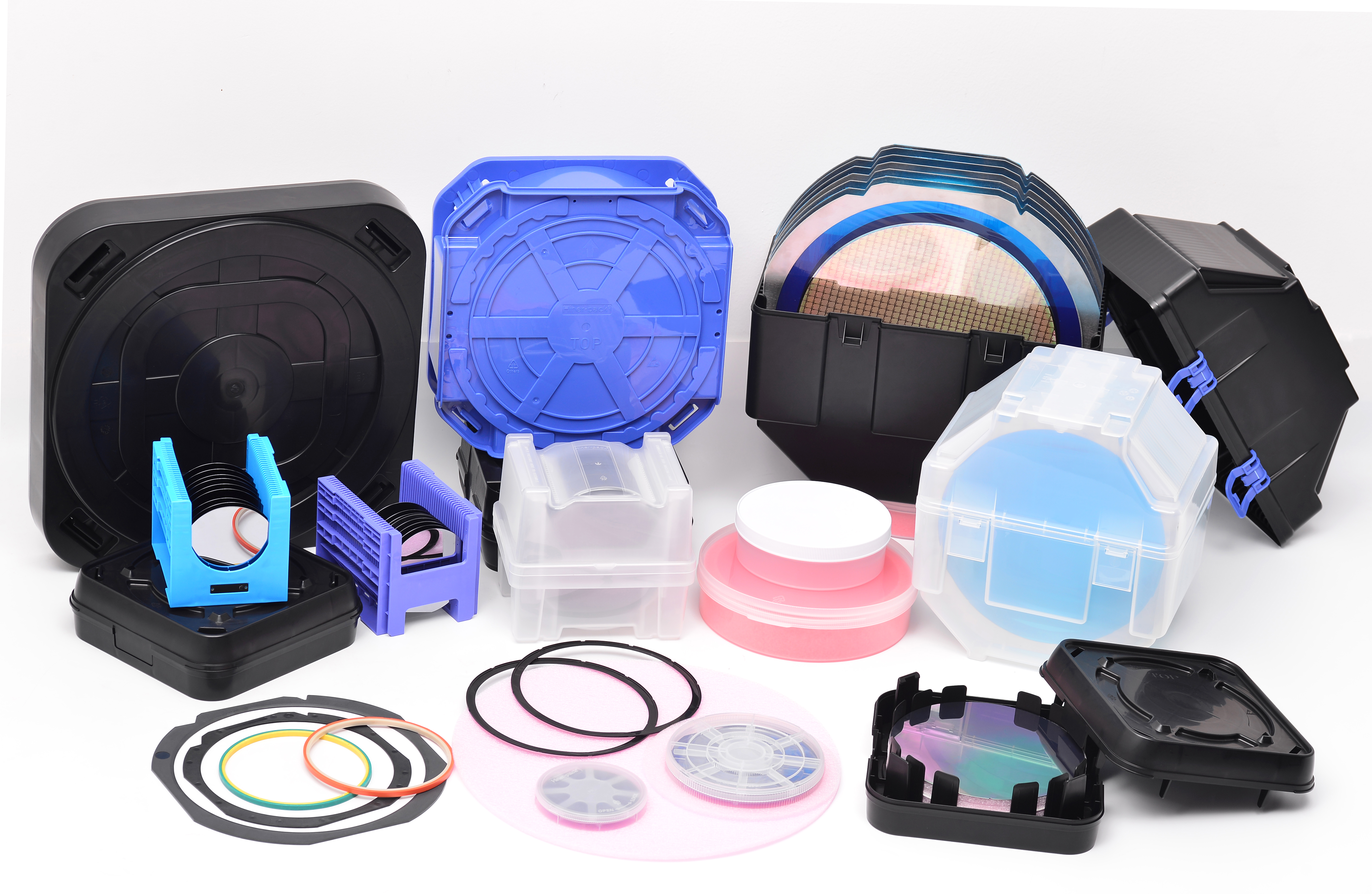
Standard wafer shippers are designed for the average, not the exceptional. They work on the assumption that all wafers, all processes, and all transport routes are identical. In reality, they are not. You may be handling 200mm wafers for power devices, ultra-fragile 300mm wafers with 10μm node geometries, or even emerging 450mm substrates for R&D. Each has unique requirements for support, pressure management, and contamination control.
A generic shipper risks:
Particle Generation: Ill-fitting supports or low-quality materials can shed contaminants.
Wafer Slippage and Breakage: Inadequate cushioning and retention can lead to catastrophic movement during transit.
Electrostatic Discharge (ESD): A poorly controlled ESD path can silently damage sensitive circuits.
Inefficient Handling: Non-optimized footprints waste valuable space in cleanrooms and shipping containers.
A truly customizable wafer shipper solution transforms this weak link into a fortified, intelligent part of your process.
Factor 1: Material Science and Contamination Control
The very substance of the shipper is your first line of defense. Not all plastics are created equal.
Static-Dissipative vs. Conductive Polymers: The choice depends on your specific ESD requirements. A high-quality customizable wafer shipper solution will offer materials with precisely controlled surface and volume resistivity to safely dissipate charge without causing a rapid discharge event.
Low Outgassing and Ionic Contamination: The materials must be certified for low levels of outgassing (to prevent clouding) and low extractable ions (like chlorides and sulfates) that can corrode or poison wafer surfaces. Suppliers like Hiner-pack typically utilize advanced polymer blends, such as carbon-loaded PEEK or specially formulated PP compounds, that meet or exceed SEMI standards.
Mechanical Strength and Durability: The material must withstand repeated use, automated handling, and the rigors of international shipping without cracking or fatiguing.
Factor 2: Precision Engineering for Wafer Size and Node
The internal architecture of the shipper is where customization proves its worth.
Wafer Diameter and Thickness: This is the baseline. A solution must perfectly accommodate 150mm, 200mm, 300mm, or 450mm wafers, and be adaptable to the varying thicknesses of finished wafers versus raw substrates.
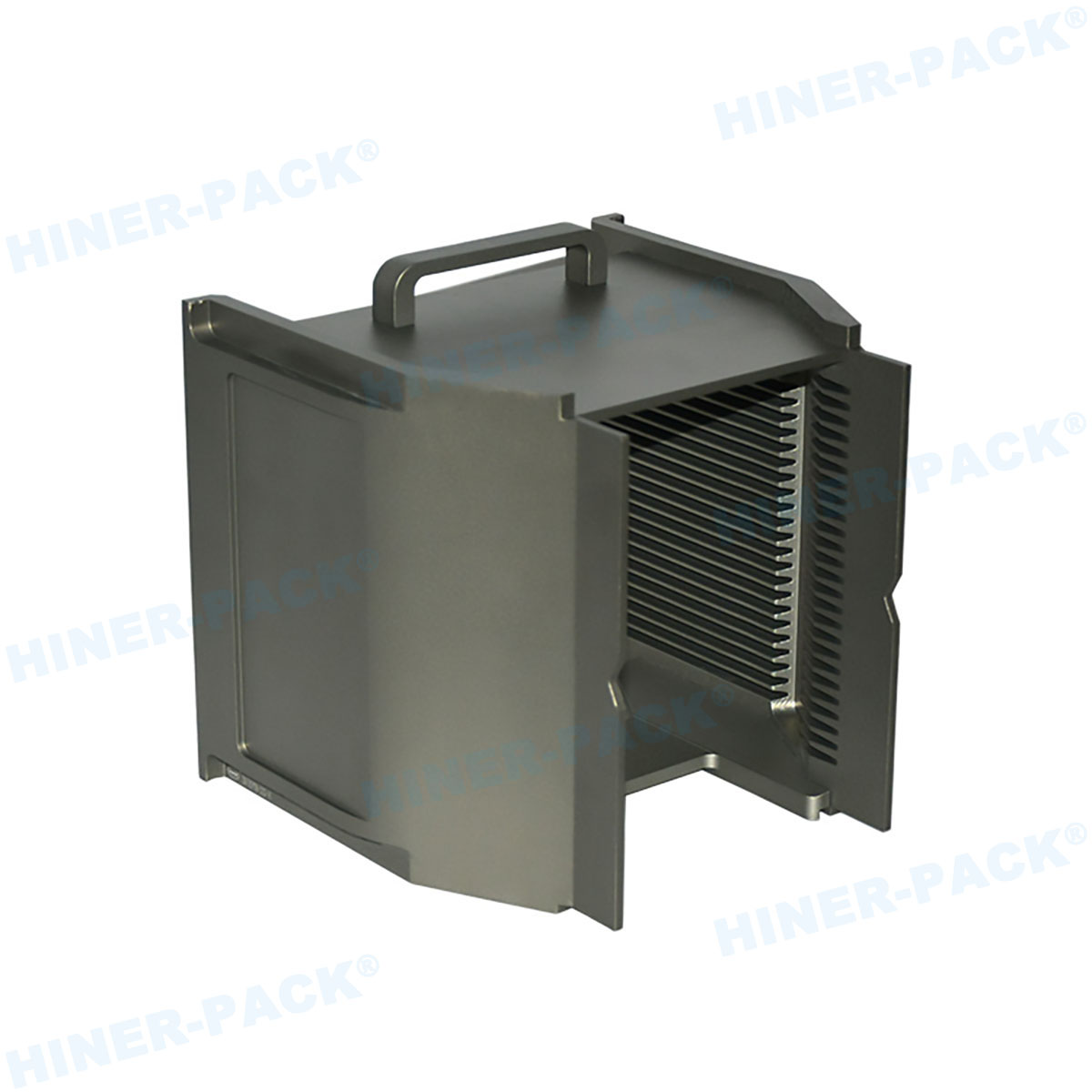
Support Geometry: For leading-edge nodes, point-of-contact is a critical concern. Custom-designed support ribs, rails, or button-type contacts can be engineered to minimize the physical touchpoints on the wafer's active surface, a feature central to a high-performance customizable wafer shipper solution.
Nesting and Stacking: Efficient storage in the fab and during transport is crucial. A well-designed shipper will allow for secure, stable stacking without putting pressure on the wafers inside the container below.
Factor 3: Advanced ESD and Physical Protection Features
Beyond basic ESD properties, advanced features are non-negotiable for high-value products.
Integrated RFI/EMI Shielding: For wafers sensitive to radio frequency or electromagnetic interference, a customizable wafer shipper solution can include metalized layers or composite structures that create a Faraday cage effect.
Cushioning and Shock Absorption: Advanced foam liners, either pre-molded or custom-die-cut, can be specified to provide a specific static crush strength and damping coefficient to protect against G-forces from drops and impacts.
Vacuum and Atmosphere Control: For wafers that are sensitive to moisture or oxygen, the shipper can be designed with ports and seals to allow for purging with inert gases like Nitrogen.
Factor 4: Automation Compatibility and Ergonomic Design
A shipper that protects the wafer but disrupts the workflow is only a partial solution.
Standardized Footprint (e.g., SEMI E1.2): Even a customizable wafer shipper solution should conform to industry-standard outer dimensions where possible to ensure compatibility with automated Material Handling Systems (MHS), stockers, and load ports.
Robotic Handling Features: This includes precisely located tooling holes, gripper ledges, and machine-readable labels (barcode, QR code, RFID pockets) that are seamlessly integrated into the customizable design.
Ergonomics for Manual Handling: For processes requiring human intervention, the design should include comfortable handholds, a balanced weight distribution, and clear, intuitive opening/closing mechanisms to reduce the risk of operator error or injury.
Factor 5: Traceability and Supply Chain Integration
In an era of Industry 4.0, the shipper can be a data carrier.
Integrated Labeling and Tracking: Custom-molded pockets for RFID tags or barcode labels protect these critical identifiers from damage or removal, enabling full lot traceability throughout the global supply chain.
Supplier Collaboration and Lead Time: When you choose a customizable wafer shipper solution, you are not just buying a product; you are entering a partnership. A supplier's ability to rapidly prototype, validate, and scale production is key. Companies like Hiner-pack often excel by working closely with clients to refine designs and ensure a reliable, just-in-time supply.
The Hiner-pack Advantage in Custom Wafer Packaging
At Hiner-pack, we understand that your wafers are not just products; they are the physical manifestation of immense intellectual and capital investment. Our approach to the customizable wafer shipper solution is rooted in deep material science and precision engineering. We don't just modify existing designs; we collaborate with you to create a purpose-built container that addresses your specific wafer types, process nodes, and logistical challenges. From advanced polymer selection to designing for flawless automation integration, our goal is to deliver a solution that provides absolute confidence, shipment after shipment.
Frequently Asked Questions (FAQs)
Q1: How much more does a customizable wafer shipper solution cost compared to a standard off-the-shelf option?
A1: The initial unit cost of a customizable wafer shipper solution is typically higher due to the engineering, prototyping, and specialized tooling involved. However, the Total Cost of Ownership (TCO) is often significantly lower. This is because a tailored solution drastically reduces costs associated with wafer loss, yield degradation, operational inefficiencies, and shipping damage, providing a strong return on investment.
Q2: What is the typical lead time for developing and receiving a new custom wafer shipper design?
A2: The lead time can vary based on complexity. A simple modification to an existing design might take 4-6 weeks. A completely new, from-scratch customizable wafer shipper solution involving new molds and material qualification can take 12-20 weeks. Reputable suppliers like Hiner-pack will provide a detailed project timeline after the initial consultation.
Q3: Can you create a custom shipper that is compatible with our existing automated material handling systems (AMHS)?
A3: Absolutely. A core tenet of an effective customizable wafer shipper solution is ensuring seamless integration into your current infrastructure. By providing the specifications of your AMHS, including robot end-effector types and stocker dimensions, the supplier can engineer the shipper's external geometry and tooling features for perfect compatibility.
Q4: What certifications and standards do your custom shipper solutions comply with?
A4: A high-quality customizable wafer shipper solution should be designed to meet relevant SEMI standards (e.g., for dimensions, ESD, and materials). Furthermore, the supplier should be able to provide material certification data sheets, test reports for outgassing (ASTM E595), and ESD performance (ESD S541). It's crucial to discuss your specific compliance requirements with your provider.
Q5: We have a unique wafer type that is extremely thin and fragile. Can a custom solution truly secure it without damage?
A5: Yes, this is a primary application for a customizable wafer shipper solution. Engineers can design specialized support structures, such as full-perimeter cradles or micro-point contacts, to distribute support forces evenly and minimize stress. They can also specify ultra-soft, low-shedding liners and precisely control the clamping force of the lid to hold the wafers immobile without applying excessive pressure.


