
In the highly precise world of semiconductor manufacturing, the journey of a silicon wafer from a bare disc to a complex integrated circuit is fraught with potential hazards. Contamination, physical stress, and electrostatic discharge (ESD) can instantly destroy millions of dollars worth of product. Often overlooked, the wafer tray and carrier solution is a first-line defense, playing a pivotal role in protecting yield and ensuring operational efficiency. Choosing the right solution isn't just a purchasing decision; it's a strategic investment in your fab's reliability.
This article delves into the five critical factors you must evaluate to select the optimal wafer tray and carrier solution for your specific application, helping you avoid costly mistakes and enhance your production line's performance.
Why Your Choice of Wafer Tray and Carrier Matters More Than You Think
Before diving into the selection criteria, it's essential to understand the high stakes. A subpar carrier can lead to:
Particle Contamination: Loose debris or outgassing from low-quality materials can settle on wafers, causing defects.
Mechanical Damage: Improper support or shock during transport can lead to micro-cracks or breakage.
Electrostatic Discharge (ESD): Without proper dissipation, static buildup can zap and destroy sensitive circuitry.
Process Incompatibility: A carrier that warps under high temperatures or reacts with chemicals can ruin an entire batch.
The consequences are not just damaged wafers but also tool downtime, increased maintenance, and significant financial loss. Therefore, a robust wafer tray and carrier solution is non-negotiable.
Factor 1: Material Composition and Purity
The foundation of any reliable carrier is its material. Not all plastics or composites are created equal.
PEEK (Polyether Ether Ketone): The gold standard for high-temperature processes. PEEK offers excellent thermal stability, low outgassing, and outstanding chemical resistance. It's ideal for applications involving CVD, etching, and other demanding thermal cycles.
PPS (Polyphenylene Sulfide): Another high-performance polymer with great thermal and chemical properties, often used as a cost-effective alternative to PEEK in certain applications.
PC (Polycarbonate) & ABS Blends: Common for general-purpose transport and storage where extreme temperatures are not a factor. They offer good impact resistance but may not suffice for front-end open cassette processes.
ESD-Safe Compounds: Specifically engineered to dissipate static charge, protecting wafers from ESD events. This is a mandatory feature for handling sensitive devices.
The key is to match the material to your process requirements. A custom wafer tray and carrier solution from a supplier like Hiner-pack often involves selecting or engineering a material grade that meets your specific purity and performance benchmarks.
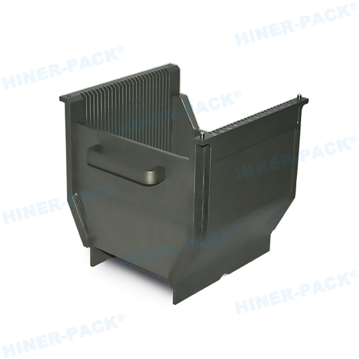
Factor 2: Design for Maximum Wafer Security and Throughput
The physical design of the tray and carrier dictates how securely wafers are held and how efficiently they can be handled.
Pocket Geometry: The wafer pockets must provide a precise, snug fit to prevent movement during transit, while minimizing contact area to reduce particle generation and stress points.
Automation Compatibility: The carrier must be designed with standardized or custom features (e.g., gripper rails, barcode locations, kinematic couplings) for seamless integration with your automated Material Handling Systems (AMHS), robots, and load ports.
Accessibility: Can operators or robots easily and safely insert and remove wafers? A good design balances security with ease of access to prevent handling errors.
Stackability and Footprint: For storage and logistics, a design that allows for secure stacking and optimizes cleanroom space is a significant advantage.
Factor 3: Compliance with Industry Standards
Adherence to industry standards ensures interoperability, safety, and quality.
SEMI Standards: Compliance with relevant SEMI standards (e.g., SEMI E1.2 for 300mm FOUPs) is crucial. These standards define critical dimensions, material properties, and performance tests, ensuring that carriers from different suppliers work interchangeably with tool load ports.
Cleanroom Class Certification: The wafer tray and carrier solution should be certified for use in your specific cleanroom class (e.g., ISO Class 1-5), guaranteeing it won't be a source of contamination.
Factor 4: The Total Cost of Ownership (TCO)
While the initial purchase price is a consideration, the Total Cost of Ownership provides a more accurate financial picture.
Initial Purchase Price: The upfront cost of the carriers.
Longevity and Durability: How many process cycles can the carrier endure before showing signs of wear? A more durable, slightly more expensive carrier may be far cheaper over its lifespan.
Maintenance and Cleaning Costs: How easy is the carrier to clean? Does it require specialized and expensive cleaning procedures? A design that facilitates quick and effective cleaning reduces downtime and operational costs.
Impact on Yield: This is the most significant factor. A high-quality carrier that prevents even a single batch failure pays for itself many times over. The cost of a carrier is negligible compared to the value of the wafers it protects.
Factor 5: Supplier Capability and Customization
Your wafer tray and carrier solution provider should be a partner, not just a vendor.
Technical Expertise: Can they provide engineering support and material science advice?
Quality Assurance: Do they have rigorous QA processes, including in-house testing for particle counts, ESD performance, and mechanical strength?
Customization Offerings: Standard solutions don't always fit unique processes. The ability to develop a custom wafer tray and carrier solution is invaluable. Whether it's a unique wafer size, a special material formulation, or a design feature for a proprietary tool, a supplier like Hiner-pack that offers engineering-level support can provide the perfect fit for your challenging requirements.
Hiner-pack: Your Partner in Advanced Wafer Handling
At Hiner-pack, we understand that precision is paramount. We don't just manufacture containers; we engineer safeguarding ecosystems for the world's most advanced technology. Our approach is collaborative. We work closely with our clients to analyze their process flow, identify potential risks, and deliver a wafer tray and carrier solution that excels in performance, durability, and cleanliness. From high-temperature PEEK carriers for demanding fab processes to ESD-safe transport trays for back-end operations, our commitment to quality and our capability for custom wafer tray and carrier solution development set us apart.
Frequently Asked Questions (FAQs)
Q1: How often should wafer trays and carriers be replaced or professionally inspected?
A1: There is no one-size-fits-all answer, as it depends on the process severity (temperature, chemicals) and handling frequency. A general guideline is a thorough inspection every 200-500 cycles. However, Hiner-pack recommends establishing a preventive maintenance schedule based on regular particle count and visual inspection data. Signs of wear, discoloration, or an increase in particle counts are clear indicators that replacement or maintenance is needed.
Q2: What is the main difference between a conductive and a dissipative wafer carrier?
A2: Both control ESD, but at different rates. Conductive materials (surface resistivity < 1 x 10^5 Ω/sq) discharge electricity very rapidly. Dissipative materials (surface resistivity between 1 x 10^5 and 1 x 10^12 Ω/sq) allow for a slower, safer discharge of static charge. For most semiconductor applications, dissipative carriers are preferred as they prevent rapid discharges that could still potentially damage sensitive components.
Q3: Can you create a custom wafer tray for a non-standard wafer size or unique geometry?
A3: Absolutely. A key strength of specialized suppliers like Hiner-pack is our ability to provide a custom wafer tray and carrier solution. We regularly engineer solutions for non-standard wafer sizes, substrates like GaAs or SiC, and specialized geometries with features like cut-outs or specific pocket arrangements to meet unique process tooling requirements.
Q4: Beyond material, what design features help minimize particle generation?
A4: Several design features are critical: smooth, radiused edges within the wafer pockets prevent scraping; minimized contact points reduce friction; and a monolithic design (as opposed to assemblies with multiple parts) eliminates gaps where particles can accumulate and be released. Hiner-pack utilizes advanced mold flow analysis and surface finishing techniques in our wafer tray and carrier solution designs to inherently minimize particle generation.
Q5: What are the cost drivers for a high-performance wafer tray and carrier solution?
A5: The primary cost drivers are the raw material (e.g., high-purity PEEK is significantly more expensive than PC), the complexity of the design and molding tool, and the level of custom wafer tray and carrier solution engineering required. Additionally, the costs associated with rigorous quality control testing, certification for industry standards, and achieving ultra-low particle counts also contribute to the final price, reflecting the higher value and protection the solution provides.


