In the semiconductor manufacturing ecosystem, the physical transport of
silicon wafers between different stages—from front-end fabrication to back-end
assembly and testing—represents a period of significant vulnerability. As wafer
diameters increase and feature sizes shrink, the sensitivity of these substrates
to mechanical vibration, electrostatic discharge (ESD), and molecular
contamination has intensified. Consequently, identifying a technically
proficient wafer
shippers supplier is no longer a peripheral procurement task; it is
a fundamental requirement for maintaining high yield rates and ensuring product
reliability.
A specialized partner like Hiner-pack understands that the
carrier is not merely a plastic container but a high-precision engineering tool.
This article examines the complex technical parameters that define
industry-leading wafer transport solutions, providing procurement engineers and
fab managers with the necessary framework to evaluate their supply chain
partners.
1. Material Science and Outgassing Dynamics
The foundation of any high-performance wafer shipper lies in the polymer
chemistry used during injection molding. When vetting a wafer shippers
supplier, the first point of analysis must be the resin grade.
Standard polymers often contain additives that can outgas Volatile Organic
Compounds (VOCs), which deposit on the wafer surface, causing unwanted
hydrophobic or hydrophilic changes that interfere with thin-film deposition or
etching processes.
Polypropylene (PP): The industry standard for many shipping
applications due to its chemical resistance and impact strength. However, the
purity of the PP must be verified via Gas Chromatography-Mass Spectrometry
(GC-MS) to ensure it meets low-outgassing requirements.
Polycarbonate (PC): Preferred for Front Opening Shipping
Boxes (FOSB) due to its superior dimensional stability and transparency, which
allows for visual or automated inspection without opening the container.
Fluoropolymers (PFA/PTFE): Reserved for the most demanding
environments where thermal stability and extreme chemical inertness are
mandatory.
A professional supplier must provide material safety data sheets (MSDS) and
certificates of compliance that detail the absence of silicone and other
hazardous substances that could lead to surface contamination.
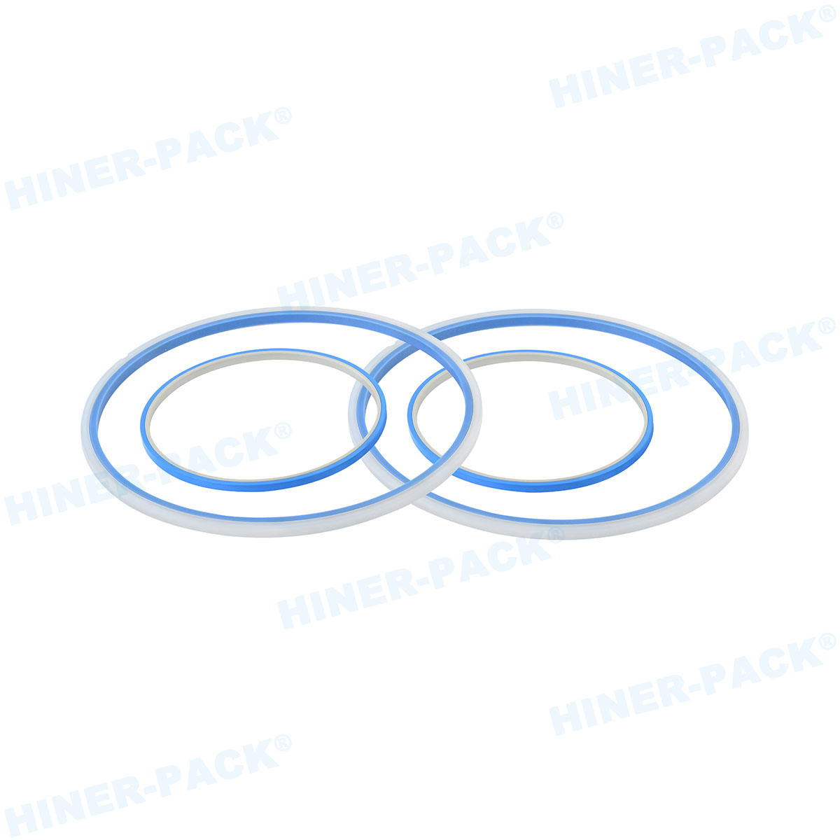
2. Electrostatic Discharge (ESD) Mitigation Strategies
Electrostatic phenomena can be catastrophic for Integrated Circuits (ICs),
particularly as gate oxides become thinner and more susceptible to dielectric
breakdown. The ability of a wafer shippers
supplier to provide consistent surface resistivity is a paramount
factor in the selection process. Static charges can attract airborne
particulates to the wafer surface or cause direct electrical damage through a
rapid discharge event.
Sophisticated shippers utilize permanent anti-static or static-dissipative
additives. Unlike topical coatings, which can migrate or wear off over time,
internal additives ensure that the surface resistivity—typically ranging from
10^5 to 10^9 ohms per square—remains stable throughout the product's lifecycle.
Testing protocols such as ASTM D257 are used to validate these electrical
properties, ensuring that the wafers remain in a Faraday cage-like environment
during transit.
3. Mechanical Engineering and Vibration Dampening
During international freight, wafers are subjected to a spectrum of vibration
frequencies. If the natural frequency of the shipper matches the environmental
vibrations, resonance can occur, leading to micro-cracks or "chipping" at the
wafer edges. A sophisticated wafer shippers
supplier employs Finite Element Analysis (FEA) to design internal
support structures that dampen these forces.
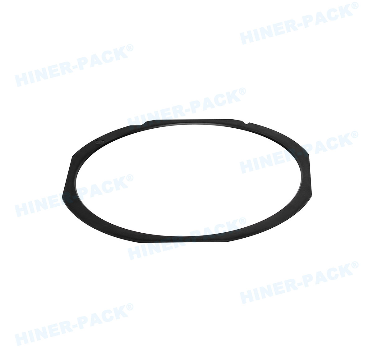
Wafer Retention Systems: The use of specialized "spring"
cushions or precision-fit slots that maintain a secure hold without applying
excessive localized pressure.
Impact Resistance: The outer shell must be robust enough to
withstand drops and external compression, protecting the brittle silicon
substrates within.
Contact Area Minimization: Modern designs focus on
contacting the wafer only within the "exclusion zone" (typically the outer 3mm
of the wafer) to protect the active die area from abrasion.
4. Contamination Control and Cleanroom Integrity
The manufacturing environment of the shipper itself is a vital metric for
quality. Hiner-pack operates under stringent cleanroom protocols to ensure that every carrier is
free from particulate matter before it reaches the customer. In the
semiconductor world, a single particle can result in a "killer defect."
Suppliers are evaluated on their ability to perform Liquid Particle Counts
(LPC) and Airborne Particle Counts (APC). Furthermore, the packaging of the
shippers—usually double or triple vacuum-sealed bagging—is necessary to prevent
contamination during the "last mile" of delivery. The integration of humidity
indicator cards and desiccant packs further ensures that the internal
micro-environment remains within the specified moisture limits, preventing
oxidation of metal pads on the wafers.
5. SEMI Standard Compliance and Automation Compatibility
As fabs transition to Industry 4.0, the compatibility of wafer shippers with
Automated Material Handling Systems (AMHS) has become a mandatory requirement.
Shippers must adhere to SEMI (Semiconductor Equipment and Materials
International) standards, such as M1, M31, and E1.7. These standards dictate the
precise dimensions of the carrier, the placement of robotic pick-up flanges, and
the kinematic coupling features.
A reliable wafer
shippers supplier ensures that their products can be seamlessly
handled by Overhead Hoist Transport (OHT) systems and Automated Guided Vehicles
(AGVs). Any deviation in the tolerances of these features can lead to robotic
"mis-picks," causing significant downtime and potential hardware damage within
the fab environment.
6. Challenges in Compound Semiconductor Packaging
The industry's shift toward Wide Bandgap (WBG) materials like Silicon Carbide
(SiC) and Gallium Nitride (GaN) has introduced new complexities. These wafers
are often heavier, more brittle, and significantly more expensive than
traditional silicon. Consequently, the packaging requirements are more
stringent.
Customized solutions for SiC wafers often include reinforced cassettes and
specialized separators that account for the unique crystalline structure and
surface roughness of the material. A supplier's ability to innovate in this
niche area is a strong indicator of their technical depth and commitment to the
evolving needs of the power electronics and 5G telecommunications sectors.
Addressing Common Industry Pain Points
One of the most persistent issues in the industry is the "out-of-box" failure
rate caused by improper packaging. Often, wafers arrive with surface scratches
or particulate contamination that was not present at the point of origin. This
highlight the gap between a standard plastic molder and a dedicated
semiconductor packaging expert. By implementing rigorous quality management
systems (QMS) and utilizing 100% automated optical inspection (AOI) for critical
dimensions, Hiner-pack addresses these risks
directly.
Another challenge is the management of specialized inventory for R&D vs.
mass production. R&D environments often require small quantities of
"coin-style" shippers for individual 100mm or 150mm wafers, while mass
production lines require bulk 300mm FOSB solutions. A versatile supplier must be
able to cater to both ends of this spectrum without compromising on the
technical specifications of either.
The Importance of Supply Chain Transparency
In an era of global uncertainty, the traceability of materials is a necessary
component of risk management. A top-tier wafer shippers
supplier provides full lot traceability, allowing fab managers to
track the raw material batch and the specific production date of every
container. This level of transparency is vital for root-cause analysis should a
contamination event occur in the production line.
Frequently Asked Questions (FAQ)
Q1: What are the primary differences between an FOSB and a standard
wafer shipper?
A1: A Front Opening Shipping Box (FOSB) is specifically designed for 300mm
wafers and is compatible with automated fab equipment. Standard wafer shippers,
such as "coin-style" or horizontal canisters, are often used for manual handling
or smaller wafer sizes (50mm-200mm) and do not typically feature the robotic
interfaces found on an FOSB.
Q2: How do you verify the ESD safety of a wafer
container?
A2: ESD safety is verified using a surface resistance meter following the
ANSI/ESD S11.11 standard. A reputable supplier will provide test reports showing
that the resistivity falls within the dissipative range (10^6 to 10^9 ohms/sq)
and that the material does not generate significant triboelectric charges during
movement.
Q3: Can these shippers be used for thin wafer
applications?
A3: Yes, but they require specific modifications. Thin wafers (e.g., those
ground down to 100 microns) are extremely flexible and prone to "oil-canning."
Shippers for thin wafers often use specialized interleaf inserts or foam
cushions to provide uniform support across the entire wafer surface.
Q4: Why is low-outgassing material mandatory for wafer
transport?
A4: Outgassing releases chemical vapors that can condense on the wafer. Even
at the parts-per-billion (ppb) level, these contaminants can lead to adhesion
failures in subsequent processing steps or cause "haze" on the wafer surface,
which negatively impacts metrology and yield.
Q5: What is the typical shelf life of a wafer shipper's anti-static
properties?
A5: Shippers made with permanent anti-static additives (integrated into the
polymer matrix) typically maintain their properties for several years, provided
they are stored away from extreme UV light and harsh chemicals. Shippers using
topical coatings may lose effectiveness after 6-12 months or after repeated
cleaning.
Conclusion and Inquiry
The selection of a packaging partner is a pivotal decision that impacts the
entire semiconductor value chain. From the initial material selection to the
final cleanroom vacuum-sealing, every step must be executed with an
understanding of the high stakes involved in wafer fabrication. As the industry
pushes the boundaries of Moore’s Law, the role of the carrier as a protector of
innovation becomes even more pronounced.
Hiner-pack remains
committed to providing the global semiconductor industry with high-purity,
ESD-safe, and SEMI-compliant transport solutions that meet the rigorous demands
of modern foundries and OSAT providers.
Are you looking to enhance your wafer protection protocols or seeking a more
reliable supply for your 200mm or 300mm production lines? Our engineering team
is available to provide technical consultations and tailored proposals based on
your specific process requirements.
Contact us today for a technical consultation and to request a formal
inquiry for your wafer shipping needs.


