In the rapidly evolving semiconductor industry, innovations in wafer technology play a pivotal role in driving advancements in electronics, from smartphones to autonomous vehicles. One such innovation is the box wafer, a specialized type of silicon wafer that has gained significant attention for its unique properties and applications. If you're involved in semiconductor design, manufacturing, or research, understanding box wafer technology is essential to staying competitive. This article delves into seven key aspects of box wafer, providing a comprehensive overview that aligns with industry standards and search trends. We'll explore its structure, benefits, manufacturing processes, and more, ensuring you have a solid grasp of why box wafer is a game-changer in the field. By the end, you'll appreciate how box wafer contributes to enhanced performance, reduced power consumption, and improved reliability in modern chip designs.
What is a Box Wafer? Understanding Its Core Definition and Structure
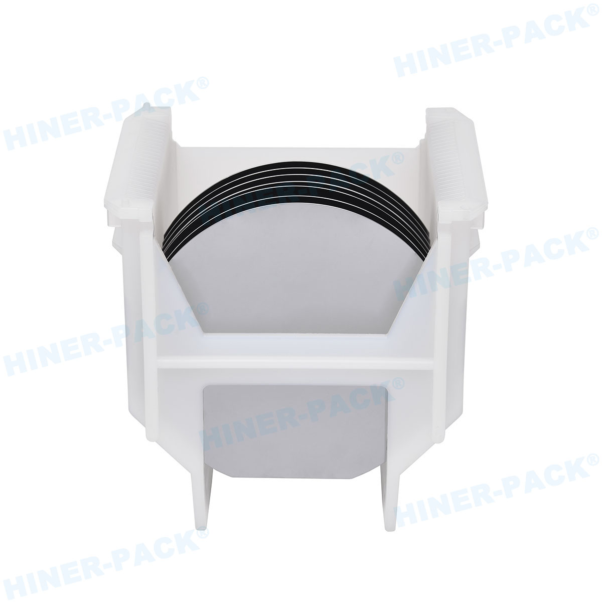
A box wafer, commonly referred to in the context of Silicon-on-Insulator (SOI) technology, is a type of semiconductor wafer that features a buried oxide (BOX) layer sandwiched between a thin top silicon layer and a bulk silicon substrate. This structure is designed to isolate the active device layer from the substrate, reducing parasitic capacitance and improving electrical performance. The term "box wafer" specifically highlights the BOX layer, which acts as an insulator, enabling faster switching speeds and lower leakage currents in transistors. Typically, the BOX layer is made of silicon dioxide (SiO2), and its thickness can vary based on application requirements, ranging from a few nanometers to several hundred nanometers. This configuration makes box wafer ideal for high-frequency and low-power applications, such as in RF devices and advanced microprocessors. By minimizing interference from the substrate, box wafer enhances overall chip efficiency, making it a cornerstone in the development of next-generation semiconductors. As the demand for energy-efficient electronics grows, the role of box wafer becomes increasingly critical in achieving performance benchmarks.
The Manufacturing Process of Box Wafer: Key Steps and Techniques
The production of box wafer involves sophisticated fabrication techniques that ensure precision and quality. One common method is the Smart Cut process, which includes bonding and layer transfer steps. First, a silicon wafer is thermally oxidized to form a thick oxide layer, which will become the BOX. Then, hydrogen ions are implanted into another wafer to create a weakened layer. The two wafers are bonded together under high pressure and temperature, after which the donor wafer is split along the implanted layer, leaving a thin silicon film on the BOX. Alternatively, SIMOX (Separation by IMplantation of OXygen) is another technique where oxygen ions are implanted into a silicon wafer and then annealed to form a buried oxide layer. Both methods require strict control over parameters like temperature, ion dose, and bonding conditions to achieve uniform layers and minimize defects. The manufacturing process for box wafer also involves post-processing steps such as chemical-mechanical polishing (CMP) to smooth the surface and ensure optimal device performance. Quality checks, including metrology and defect inspection, are crucial to verify the integrity of the BOX layer and the overall wafer structure. This meticulous process underscores why box wafer is often more expensive than traditional bulk silicon wafers but offers superior performance in demanding applications.
Advantages of Box Wafer in Semiconductor Applications
Box wafer provides numerous advantages that make it a preferred choice in various semiconductor applications. Firstly, it significantly reduces power consumption by minimizing leakage currents, which is vital for battery-powered devices like smartphones and IoT sensors. The insulating BOX layer prevents current from flowing into the substrate, leading to higher efficiency and longer battery life. Secondly, box wafer enhances performance in high-frequency circuits, such as those used in 5G communication systems, by reducing parasitic capacitance and enabling faster signal propagation. Thirdly, it improves radiation hardness, making box wafer suitable for aerospace and automotive electronics where reliability under harsh conditions is paramount. Additionally, box wafer supports the integration of multiple technologies on a single chip, such as in system-on-chip (SoC) designs, by providing better isolation between components. This reduces crosstalk and improves signal integrity. Moreover, the use of box wafer can lead to smaller transistor sizes and higher packing densities, aligning with the industry's push toward Moore's Law scaling. Overall, these benefits make box wafer an enabler of innovation in areas like artificial intelligence, edge computing, and advanced driver-assistance systems (ADAS).
Comparison of Box Wafer with Other Wafer Types
When comparing box wafer to other wafer types, such as bulk silicon wafers or epitaxial wafers, several distinctions emerge. Bulk silicon wafers are the most common and cost-effective option but suffer from higher leakage currents and parasitic effects due to the lack of an insulating layer. In contrast, box wafer's BOX layer provides superior isolation, resulting in better performance for low-power and high-speed applications. Epitaxial wafers, which have a grown silicon layer on a substrate, offer improved purity and defect control but do not provide the same level of electrical isolation as box wafer. For instance, in RF applications, box wafer outperforms epitaxial wafers by reducing substrate losses and enabling higher quality factors. However, box wafer tends to be more expensive and complex to manufacture, which can be a drawback for cost-sensitive projects. Another comparison point is with fully depleted silicon-on-insulator (FD-SOI) wafers, which are a subset of box wafer technology; FD-SOI leverages ultra-thin layers for even better control over short-channel effects in transistors. Ultimately, the choice between box wafer and other types depends on factors like application requirements, budget, and performance targets. In summary, box wafer stands out for its balanced trade-offs in isolation, power efficiency, and integration capabilities.
Current Trends and Future Outlook for Box Wafer Technology
The box wafer market is experiencing robust growth, driven by trends such as the proliferation of 5G networks, the Internet of Things (IoT), and electric vehicles. According to industry reports, the global SOI wafer market, which includes box wafer, is projected to expand at a compound annual growth rate (CAGR) of over 10% in the coming years. Key players like Soitec, GlobalFoundries, and STMicroelectronics are investing in advanced box wafer technologies to meet the demand for energy-efficient chips. One emerging trend is the adoption of box wafer in artificial intelligence and machine learning hardware, where low power and high speed are critical. Additionally, the shift toward more sustainable electronics is pushing manufacturers to explore box wafer for reducing carbon footprints through improved efficiency. Looking ahead, research is focused on enhancing the BOX layer with materials like high-k dielectrics to further boost performance. The integration of box wafer with 3D packaging techniques is also gaining traction, enabling higher density and functionality in compact devices. As semiconductor nodes shrink below 10nm, box wafer is expected to play a vital role in overcoming scaling challenges, ensuring its relevance in the future of electronics.
Challenges and Solutions in Box Wafer Implementation
Despite its benefits, box wafer faces several challenges that need addressing for widespread adoption. One major issue is the higher cost compared to bulk silicon wafers, primarily due to complex manufacturing processes like Smart Cut or SIMOX. This can limit its use in cost-sensitive applications. To mitigate this, manufacturers are optimizing production techniques to reduce waste and improve yield. For example, recycling substrates and using larger wafer diameters (e.g., 300mm) can lower per-wafer costs. Another challenge is defect management, such as voids or dislocations in the BOX layer, which can impair device performance. Advanced metrology tools and in-process monitoring are being employed to detect and correct defects early. Thermal management is also a concern, as the BOX layer can act as a thermal barrier, leading to overheating in high-power devices. Solutions include incorporating thermal vias or using materials with better thermal conductivity in the stack. Furthermore, design complexity requires specialized expertise, which can be a barrier for smaller companies. Collaboration between foundries and design houses, along with educational initiatives, is helping to bridge this gap. By tackling these challenges, the industry is poised to unlock the full potential of box wafer in next-generation semiconductors.
Environmental and Economic Impact of Box Wafer Adoption
The adoption of box wafer has significant environmental and economic implications. From an environmental perspective, box wafer contributes to sustainability by enabling energy-efficient devices that consume less power, thereby reducing greenhouse gas emissions. For instance, in data centers, chips built on box wafer can lower cooling requirements and overall energy usage. However, the manufacturing process itself involves high energy consumption and chemical usage, which poses environmental risks. To address this, companies are adopting greener practices, such as using renewable energy in fabs and recycling water and materials. Economically, the box wafer market is creating opportunities for job growth and innovation, particularly in regions with strong semiconductor ecosystems like Asia and North America. The higher initial costs of box wafer are often offset by long-term savings through improved product performance and reliability. Moreover, as governments worldwide invest in semiconductor self-sufficiency, box wafer technology is receiving funding and support, driving economic resilience. In summary, while there are trade-offs, the overall impact of box wafer is positive, aligning with global goals for technological advancement and sustainability.
In conclusion, box wafer represents a transformative technology in the semiconductor industry, offering unparalleled advantages in performance, power efficiency, and integration. From its unique structure with a buried oxide layer to its role in cutting-edge applications like 5G and AI, box wafer is shaping the future of electronics. By understanding its manufacturing intricacies, benefits, and challenges, professionals can make informed decisions to leverage this technology effectively. As trends continue to evolve, box wafer will likely remain at the forefront of innovation, driving progress toward smarter, more efficient devices. Whether you're an engineer, researcher, or business leader, keeping abreast of box wafer developments is crucial for staying ahead in this competitive field.
Frequently Asked Questions (FAQ)
Q1: What is the primary purpose of a box wafer in semiconductor devices?
A1: The primary purpose of a box wafer is to provide electrical isolation through its buried oxide (BOX) layer, which reduces parasitic capacitance and leakage currents, leading to improved performance and lower power consumption in devices like transistors and integrated circuits.
Q2: How does box wafer differ from traditional bulk silicon wafers?
A2: Box wafer differs from traditional bulk silicon wafers by incorporating an insulating BOX layer between the active silicon and the substrate, which enhances isolation and reduces unwanted electrical effects. In contrast, bulk silicon wafers lack this layer, making them more prone to leakage and slower speeds in high-frequency applications.
Q3: What are the common manufacturing methods for box wafer?
A3: Common manufacturing methods for box wafer include the Smart Cut process, which involves bonding and layer transfer, and the SIMOX technique, where oxygen ions are implanted and annealed to form the buried oxide layer. Both methods require precise control to ensure high-quality wafers.
Q4: In which applications is box wafer most beneficial?
A4: Box wafer is most beneficial in applications requiring low power consumption and high performance, such as RF communication systems, Internet of Things (IoT) devices, automotive electronics, and advanced microprocessors. It is also favored in radiation-sensitive environments like aerospace.
Q5: What are the main challenges associated with using box wafer?
A5: The main challenges include higher manufacturing costs compared to bulk wafers, potential defects in the BOX layer, thermal management issues due to the insulating layer, and the need for specialized design expertise. Solutions involve process optimization, advanced metrology, and thermal integration techniques.
Q6: How is the box wafer market expected to evolve in the next decade?
A6: The box wafer market is expected to grow significantly, driven by demand for energy-efficient electronics and advancements in 5G, AI, and electric vehicles. Innovations in materials and packaging, along with increased investment, will likely expand its adoption across various sectors.
Q7: Can box wafer be used in combination with other semiconductor technologies?
A7: Yes, box wafer can be integrated with other technologies such as 3D packaging, FinFET transistors, and FD-SOI to enhance performance and functionality. This compatibility allows for versatile designs in complex systems-on-chip (SoCs) and emerging computing architectures.


