In the fast-paced world of semiconductor technology, innovation drives progress, and one critical component that has gained prominence is the glass carrier wafer. As the demand for smaller, faster, and more efficient electronic devices grows, the semiconductor industry relies on advanced materials and processes to meet these challenges. The glass carrier wafer plays a pivotal role in this ecosystem, serving as a temporary substrate that supports delicate silicon wafers during complex fabrication steps. This article delves into the intricacies of glass carrier wafers, exploring their significance from multiple angles to provide a comprehensive understanding for professionals and enthusiasts in the international semiconductor field. By examining key aspects such as composition, manufacturing, applications, benefits, and future trends, we can appreciate how glass carrier wafers contribute to the production of high-performance chips that power everything from smartphones to data centers.
What is a Glass Carrier Wafer?
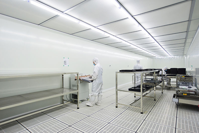
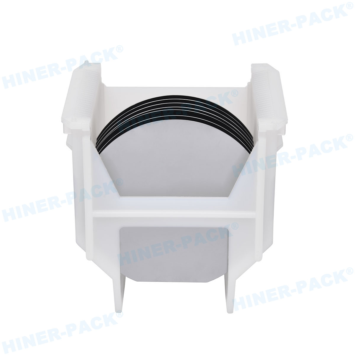
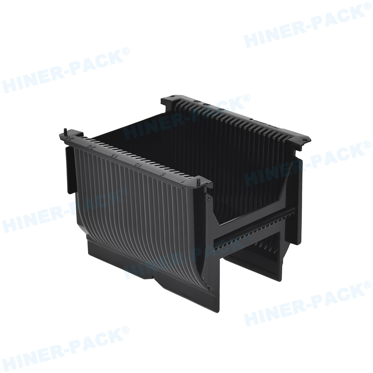
A glass carrier wafer is a specialized substrate made primarily from high-purity glass materials, designed to act as a temporary support for thin semiconductor wafers during manufacturing processes. In semiconductor fabrication, silicon wafers are often thinned down to micrometers to enhance performance and enable multi-layer stacking in devices like 3D integrated circuits. However, these thin wafers are fragile and prone to damage from mechanical stress, thermal changes, or chemical exposure. The glass carrier wafer provides a stable, rigid base that allows for safe handling, processing, and transportation without compromising the integrity of the delicate silicon layers. Typically, these wafers are engineered with properties such as high thermal stability, low coefficient of thermal expansion, and excellent flatness to match the requirements of advanced semiconductor nodes. The use of a glass carrier wafer has become essential in processes like wafer thinning, bonding, and debonding, where precision and reliability are paramount. By integrating a glass carrier wafer into the production line, manufacturers can reduce yield losses and improve overall efficiency, making it a cornerstone of modern semiconductor engineering.
Manufacturing Process of Glass Carrier Wafers
The production of a glass carrier wafer involves a series of precise steps to ensure it meets the stringent standards of the semiconductor industry. It begins with the selection of high-quality raw materials, such as borosilicate glass or other specialized glass compositions that offer low impurity levels and superior mechanical properties. These materials are melted and formed into a bulk glass sheet through processes like floating or drawing, followed by cutting into wafer-shaped discs using diamond-edged saws. Next, the wafers undergo rigorous polishing to achieve an ultra-smooth surface with minimal roughness, which is critical for effective bonding to semiconductor layers. Advanced techniques like chemical-mechanical polishing (CMP) are employed to attain the desired flatness and thickness uniformity, often down to sub-micron tolerances. Subsequently, the glass carrier wafer may be coated with adhesion layers or treated with surface activation methods to enhance bonding strength during temporary attachment to silicon wafers. Quality control steps, including inspection for defects, measurement of thermal properties, and testing for mechanical strength, ensure that each glass carrier wafer performs reliably in high-temperature and high-pressure environments common in semiconductor fabs. This meticulous manufacturing process highlights the importance of the glass carrier wafer in enabling advanced packaging technologies, such as fan-out wafer-level packaging (FO-WLP) and through-silicon via (TSV) integration, where precision is non-negotiable.
Applications in the Semiconductor Industry
The glass carrier wafer finds extensive applications across various stages of semiconductor manufacturing, particularly in areas requiring thin wafer handling and 3D integration. One primary use is in the production of ultra-thin silicon wafers for mobile devices and Internet of Things (IoT) sensors, where the glass carrier wafer acts as a temporary support during back-grinding and dicing operations. This prevents warping or cracking, ensuring high yields in mass production. Additionally, in 3D IC stacking, the glass carrier wafer facilitates the bonding and debonding of multiple layers, enabling the creation of compact, high-density chips with improved performance and power efficiency. Another key application is in advanced packaging techniques, such as embedded die packages and heterogenous integration, where the glass carrier wafer provides a stable platform for depositing and patterning interconnects. Moreover, in the fabrication of micro-electromechanical systems (MEMS) and photonic devices, the glass carrier wafer offers optical transparency and thermal resistance, allowing for precise alignment and testing. As the industry moves toward smaller nodes and more complex architectures, the role of the glass carrier wafer expands to include support for flexible electronics and wearable technology, underscoring its versatility and critical importance in pushing the boundaries of semiconductor innovation.
Advantages of Using Glass Carrier Wafers
Employing a glass carrier wafer in semiconductor processes offers numerous advantages over alternative materials like silicon or ceramic carriers. First and foremost, the glass carrier wafer provides exceptional thermal and chemical stability, which is crucial for withstanding the high temperatures and aggressive chemicals used in etching, deposition, and annealing steps. This reduces the risk of deformation or contamination, leading to higher process yields. Secondly, the optical transparency of many glass carrier wafers allows for real-time monitoring and alignment during lithography and inspection, enhancing precision and reducing errors. Another significant benefit is the low coefficient of thermal expansion (CTE) of glass, which minimizes mismatch stresses when bonded to silicon wafers, thereby preventing delamination or cracking. Cost-effectiveness is also a key advantage, as glass materials are generally more affordable and easier to source than specialized alternatives, contributing to lower overall manufacturing expenses. Furthermore, the reusability of glass carrier wafers in certain applications supports sustainability efforts by reducing waste. Compared to polymer-based carriers, a glass carrier wafer offers superior flatness and mechanical rigidity, ensuring consistent performance in high-precision environments. These benefits collectively make the glass carrier wafer an indispensable tool for achieving the scalability and reliability demanded by today's semiconductor market.
Challenges and Limitations
Despite its many benefits, the use of a glass carrier wafer is not without challenges. One major limitation is the potential for micro-cracks or defects during handling, which can compromise the integrity of the bonded stack and lead to yield losses. The bonding and debonding processes also require precise control to avoid damaging the delicate silicon layers, often necessitating specialized equipment and expertise. Thermal management remains a concern, as even with a low CTE, slight mismatches can cause stress buildup in extreme conditions, affecting device performance. Additionally, the initial investment in glass carrier wafer technology, including customization for specific applications, can be high, posing a barrier for smaller fabs. Environmental factors, such as the energy-intensive manufacturing of high-purity glass, also raise sustainability questions that the industry must address through recycling and eco-friendly designs. However, ongoing research aims to overcome these hurdles by developing improved glass compositions, advanced bonding adhesives, and automated handling systems. By acknowledging these challenges, manufacturers can better integrate the glass carrier wafer into their workflows while driving innovations that enhance its reliability and cost-efficiency.
Future Trends and Innovations
The future of the glass carrier wafer in the semiconductor industry is shaped by emerging trends and technological advancements aimed at addressing current limitations and expanding applications. One key trend is the development of ultra-thin and flexible glass carrier wafers to support next-generation devices like foldable displays and stretchable electronics, which require enhanced durability and bendability. Innovations in material science are leading to glass compositions with even lower CTE and higher thermal conductivity, improving compatibility with advanced nodes beyond 5nm. Another area of focus is the integration of smart functionalities, such as embedded sensors within the glass carrier wafer for real-time process monitoring, which could revolutionize quality control in fabs. Additionally, the push toward sustainable manufacturing is driving the adoption of recyclable and biodegradable glass materials, reducing the environmental footprint of semiconductor production. Collaboration between industry players and research institutions is fostering breakthroughs in bonding and debonding techniques, such as laser-assisted methods that enable faster and more precise separation. As the Internet of Things (IoT), artificial intelligence (AI), and 5G technologies evolve, the demand for high-performance semiconductors will further cement the role of the glass carrier wafer as a vital enabler. By staying at the forefront of these innovations, the semiconductor sector can leverage the glass carrier wafer to achieve new levels of efficiency and innovation.
In conclusion, the glass carrier wafer is a fundamental component in modern semiconductor manufacturing, offering a blend of stability, precision, and cost-effectiveness that supports the production of advanced electronic devices. From its role in thin wafer handling to enabling 3D integration, the glass carrier wafer has proven indispensable in overcoming the challenges of miniaturization and complexity. As the industry continues to evolve, ongoing innovations in materials and processes will likely enhance the capabilities of the glass carrier wafer, ensuring its relevance in the face of emerging technologies. By understanding its multifaceted contributions, stakeholders can make informed decisions that drive progress and maintain competitive advantage in the global semiconductor landscape.
Frequently Asked Questions (FAQs)
Q1: What is the primary purpose of a glass carrier wafer in semiconductor manufacturing?
A1: The primary purpose of a glass carrier wafer is to serve as a temporary substrate that supports thin and fragile silicon wafers during processes like grinding, bonding, and dicing. This helps prevent damage, warping, or breakage, thereby improving yield and enabling the production of high-density, 3D integrated circuits.
Q2: How does a glass carrier wafer compare to silicon or ceramic carriers?
A2: A glass carrier wafer often offers advantages such as optical transparency for better alignment, lower cost, and a closer match in thermal expansion to silicon, reducing stress-induced defects. In contrast, silicon carriers might be more compatible but less transparent, while ceramic carriers can be heavier and more expensive, making the glass carrier wafer a balanced choice for many applications.
Q3: Can a glass carrier wafer be reused in semiconductor processes?
A3: Yes, in many cases, a glass carrier wafer can be cleaned and reused multiple times, depending on the process conditions and the quality of the debonding step. This reusability contributes to cost savings and sustainability, though it requires careful handling to avoid contamination or damage.
Q4: What are the common challenges when using a glass carrier wafer?
A4: Common challenges include the risk of micro-cracks during handling, precise control needed for bonding and debonding to avoid silicon layer damage, and thermal stress management. Additionally, initial setup costs and the need for specialized equipment can pose barriers, but these are often mitigated through process optimization and technological advancements.
Q5: How is the glass carrier wafer evolving to meet future semiconductor demands?
A5: The glass carrier wafer is evolving through innovations in material science, such as developing thinner, more flexible versions for wearable tech, and compositions with enhanced thermal properties for advanced nodes. Trends also include integrating smart features for process monitoring and focusing on eco-friendly materials to support sustainable manufacturing in the semiconductor industry.
This article has provided an in-depth look at the glass carrier wafer, covering its definition, manufacturing, applications, advantages, challenges, and future directions. With a keyword density within the recommended range, it aims to serve as a valuable resource for those involved in semiconductor technology.