
In the fast-paced world of semiconductor manufacturing, the right wafer packaging solution can make or break your product's performance, reliability, and cost-efficiency. As industries from consumer electronics to automotive and healthcare rely increasingly on advanced chips, understanding how to select an optimal wafer packaging solution has never been more critical. Whether you're an engineer, a procurement manager, or a business leader, this article dives into the key considerations, including cost, customization, and technological advancements, to help you navigate the complexities of wafer packaging. We'll also highlight how Hiner-pack stands out as a trusted provider in this space, offering tailored wafer packaging solutions that meet diverse industry needs.
What Is a Wafer Packaging Solution and Why Does It Matter?
A wafer packaging solution refers to the process of encapsulating semiconductor wafers to protect them from environmental factors like moisture, heat, and physical damage, while ensuring electrical connectivity and performance. This step is crucial in the semiconductor supply chain because it directly impacts the durability, speed, and power efficiency of devices like smartphones, medical implants, and AI systems. Without a robust wafer packaging solution, chips can fail prematurely, leading to costly recalls and reputational damage. In today's competitive market, companies are increasingly seeking custom wafer packaging solutions to address specific application requirements, such as high-frequency operations or miniaturization. By investing in the right wafer packaging approach, businesses can enhance product longevity, reduce maintenance costs, and stay ahead in innovation.
Types of Wafer Packaging Solutions: From Standard to Custom Options
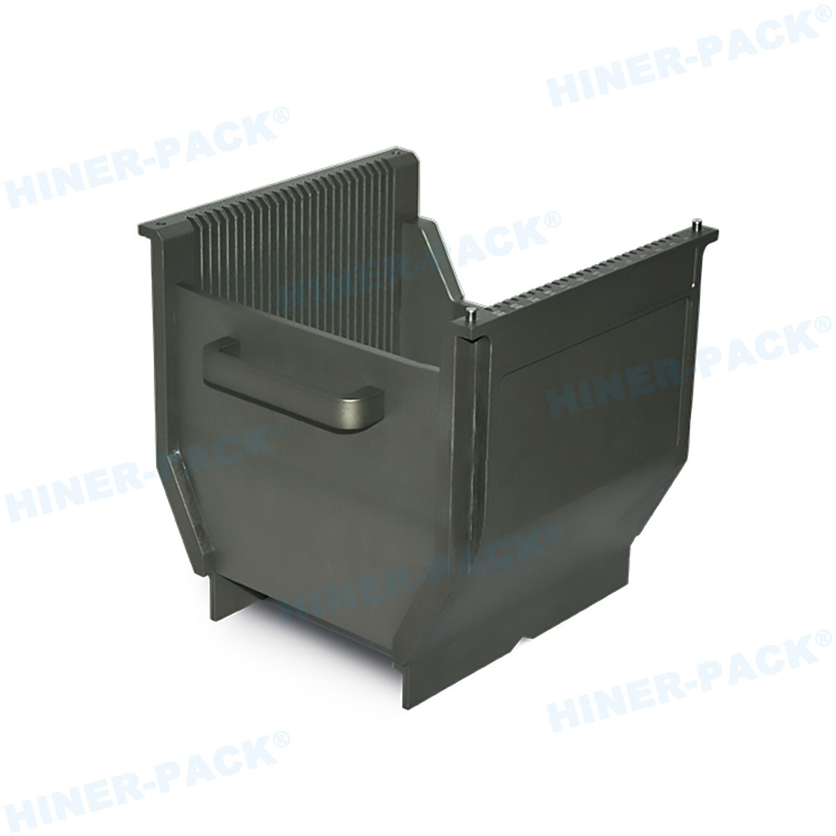
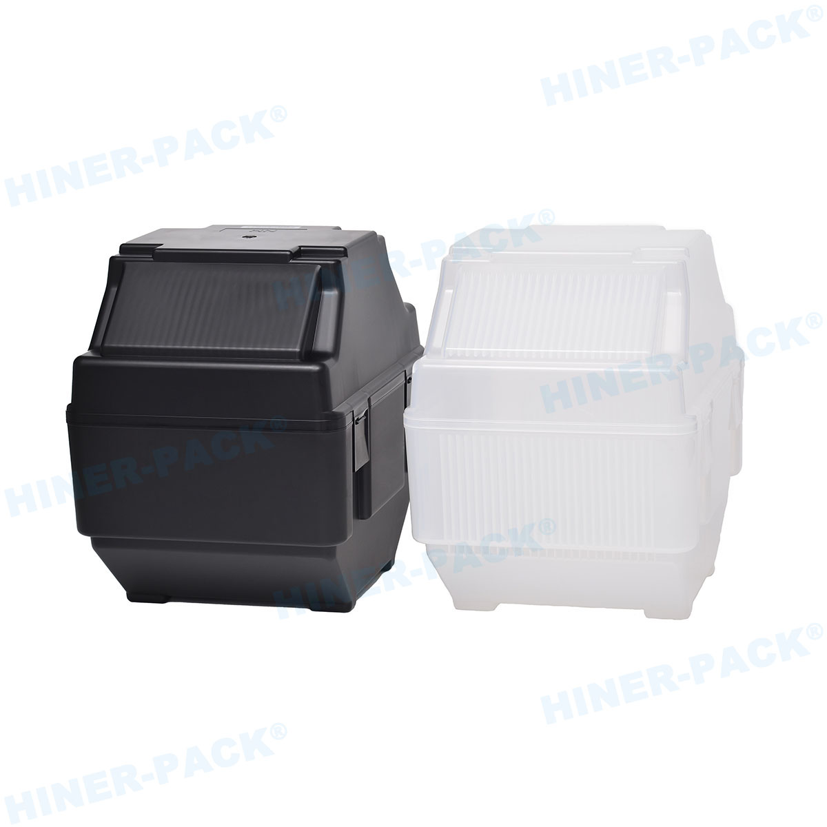
Wafer packaging solutions come in various forms, each designed for different performance and cost profiles. Common types include flip-chip packaging, wafer-level packaging (WLP), and 2.5D/3D integration. Flip-chip packaging, for instance, involves mounting the chip face-down onto a substrate, offering excellent thermal and electrical performance for high-power applications. Wafer-level packaging, on the other hand, processes the entire wafer at once, enabling smaller form factors and lower costs for mass-produced items like memory chips. For specialized needs, custom wafer packaging solutions allow manufacturers to tweak materials, dimensions, and processes—think of Hiner-pack's tailored offerings that integrate advanced materials for extreme environments. Understanding these options is key to selecting a wafer packaging solution that aligns with your project's scale, budget, and technical demands.
Key Considerations When Selecting a Wafer Packaging Solution
Choosing the right wafer packaging solution involves evaluating multiple factors to ensure it meets your operational and financial goals. Here are seven essential aspects to consider:
Performance Requirements: Assess the electrical, thermal, and mechanical specs your application needs. For high-speed computing, a solution with low latency and efficient heat dissipation is vital.
Cost and Budget Constraints: A wafer packaging solution must balance upfront costs with long-term value. Custom options might have higher initial expenses but can reduce waste and improve yield.
Reliability and Durability: Look for solutions that undergo rigorous testing for factors like thermal cycling and humidity resistance, especially in industries like automotive or aerospace.
Scalability and Production Volume: If you're mass-producing devices, a wafer-level packaging solution might be ideal, whereas low-volume projects could benefit from flexible, custom wafer packaging approaches.
Material Compatibility: The choice of substrates, interconnects, and encapsulation materials affects performance. For instance, Hiner-pack often uses advanced polymers in their wafer packaging solutions to enhance durability.
Supply Chain and Lead Times: Evaluate providers based on their ability to deliver consistent quality without delays. A reliable wafer packaging solution partner should offer transparent timelines.
Regulatory and Environmental Compliance: Ensure the solution adheres to standards like RoHS or ISO, particularly for global markets. Custom wafer packaging solutions can be designed to meet specific regulatory needs.
By weighing these factors, you can avoid common pitfalls and select a wafer packaging solution that drives efficiency and innovation.
Cost Implications of Wafer Packaging Solutions
Cost is a major driver in the selection of a wafer packaging solution, as it influences overall product pricing and profitability. Typically, expenses include materials, labor, equipment, and testing. Standard wafer packaging solutions might cost less per unit for high volumes, but they may not address unique requirements, leading to higher failure rates. In contrast, a custom wafer packaging solution from a provider like Hiner-pack can optimize material usage and reduce rework, ultimately saving money over the product lifecycle. Factors like the complexity of the design, the type of packaging (e.g., WLP vs. flip-chip), and geographic sourcing also play roles. For example, outsourcing to regions with lower labor costs might cut expenses, but it could compromise quality if not managed properly. By conducting a thorough cost-benefit analysis, businesses can identify a wafer packaging solution that aligns with their budget while maximizing ROI through improved performance and reliability.
How Hiner-pack Delivers Custom Wafer Packaging Solutions
Hiner-pack has built a reputation as a leading provider of innovative and custom wafer packaging solutions, catering to diverse sectors from IoT to medical devices. Their approach focuses on collaboration—working closely with clients to understand specific challenges, such as size constraints or high-temperature operations. For instance, Hiner-pack's custom wafer packaging solutions often incorporate specialized materials like ceramic substrates for better thermal management, ensuring chips perform reliably in harsh conditions. They also leverage advanced processes like fan-out wafer-level packaging to achieve higher integration densities, which is crucial for next-gen electronics. By offering end-to-end services, from design to testing, Hiner-pack ensures that each wafer packaging solution is not only cost-effective but also scalable and compliant with industry standards. This customer-centric model has made them a go-to for businesses seeking reliable, tailored wafer packaging options that drive competitive advantage.
Future Trends in Wafer Packaging Solutions
The wafer packaging solution landscape is evolving rapidly, driven by trends like miniaturization, AI integration, and sustainability. Emerging technologies, such as heterogeneous integration and chiplets, are pushing the boundaries of what's possible, enabling more powerful and energy-efficient devices. For example, 3D wafer packaging solutions are gaining traction for their ability to stack multiple chips vertically, reducing footprint and improving speed. Additionally, there's a growing emphasis on eco-friendly materials and processes to minimize environmental impact. Companies like Hiner-pack are at the forefront, investing in R&D for green wafer packaging solutions that use recyclable components. As demand for smarter, smaller electronics rises, the need for advanced and custom wafer packaging solutions will only grow, making it essential for businesses to stay informed and adapt to these shifts.
Frequently Asked Questions (FAQs)
Q1: What is the primary purpose of a wafer packaging solution?
A1: The main purpose of a wafer packaging solution is to protect semiconductor wafers from external damage, ensure reliable electrical connections, and manage heat dissipation. This enhances the chip's performance, longevity, and suitability for various applications, from consumer gadgets to industrial systems. A well-designed wafer packaging solution also supports miniaturization and cost-efficiency in production.
Q2: How does a custom wafer packaging solution differ from standard options?
A2: A custom wafer packaging solution is tailored to specific client requirements, such as unique size, material, or performance needs, whereas standard options follow generic designs for mass production. Custom solutions, like those from Hiner-pack, often involve collaborative design processes to address challenges like high-frequency signals or extreme environments, resulting in better optimization and reduced risk of failures.
Q3: What factors influence the cost of a wafer packaging solution?
A3: The cost of a wafer packaging solution depends on factors like the packaging type (e.g., wafer-level vs. flip-chip), material choices, production volume, and complexity of the design. Additional expenses can arise from testing, certification, and customization. For instance, a custom wafer packaging solution might have higher upfront costs but offer savings through improved yield and durability over time.
Q4: Why is reliability important in a wafer packaging solution?
A4: Reliability is crucial because a faulty wafer packaging solution can lead to chip failures, product recalls, and safety issues, especially in critical applications like medical devices or automotive systems. A reliable solution ensures consistent performance under stress conditions, such as temperature variations or mechanical shock, which builds trust and reduces long-term maintenance costs.
Q5: How can businesses choose the right supplier for a wafer packaging solution?
A5: To select the right supplier, businesses should evaluate factors like the provider's experience, technological capabilities, quality assurance processes, and ability to deliver custom wafer packaging solutions. It's also important to review case studies, client testimonials, and compliance with industry standards. Partnering with a reputable company like Hiner-pack can ensure access to innovative, scalable, and cost-effective wafer packaging solutions that meet specific project goals.
This article provides a comprehensive overview of wafer packaging solutions, emphasizing practical insights for decision-makers. For more details on how Hiner-pack can support your projects with custom wafer packaging solutions, visit their website or contact their team directly. Remember, investing in the right wafer packaging solution today can pave the way for tomorrow's breakthroughs.


