
The semiconductor industry operates at nanometer scales, where a single organic residue or metallic ion on a wafer surface can ruin an entire batch. Traditional analytical methods such as ICP-MS or optical surface scanning often lack the resolution or chemical specificity needed for trace-level identification of charged contaminants. This is where gel box electrophoresis provides a paradigm shift – a technique borrowed from molecular biology but adapted with rigorous modifications for wafer contamination analysis. In this article, we examine the technical foundations, implementation workflows, and performance benchmarks of gel box electrophoresis for semiconductor fabs, supported by best-in-class sample handling from Hiner-pack.
1. The Principle: Why Gel Box Electrophoresis Fits Wafer Contamination Detection
At its core, gel box electrophoresis separates charged species under an electric field within a sieving gel matrix. For semiconductor applications, the target analytes include metal ions (Fe, Cu, Ni, Cr), quaternary ammonium compounds from photoresist residues, and anionic surfactants from cleaning steps. The wafer surface is extracted using a controlled volume of ultra-pure buffer, and the extract is loaded into a specialized gel box electrophoresis unit. Charged contaminants migrate at rates proportional to their charge-to-mass ratio, forming discrete bands that can be visualized by staining or coupled with mass spectrometry.
Compared to conventional total-reflection X-ray fluorescence (TXRF), gel box electrophoresis offers molecular specificity: it not only quantifies elemental composition but also distinguishes between free ions and complexed species – a critical parameter for etching and CMP processes. The method complies with SEMI M53-1108 guidelines for trace contaminant analysis when executed with proper cleanroom protocols.
2. Technical Parameters of a Production-Ready Gel Box Electrophoresis System
To achieve repeatable detection limits below 1 ppb (parts per billion) on 300 mm wafers, the gel box electrophoresis setup must be optimized. Key parameters include:
Gel composition: High-resolution polyacrylamide (10–15% T) for small ions versus agarose (0.8–1.5%) for larger organic aggregates. For wafer contaminants, 12% acrylamide with 0.1% SDS provides optimal resolution for metal–organic complexes.
Running buffer: Tris-borate-EDTA (TBE) or Tris-glycine, adjusted to pH 8.3 to maintain ion solubility. EDTA chelates background metals, reducing noise.
Voltage and current: Constant voltage 120–150 V for 45–90 minutes. Field strength above 10 V/cm may cause Joule heating, distorting bands.
Sample loading volume: 20–50 µL per well, using gel combs that produce wells compatible with wafer extract concentration.
Detection method: Silver staining for nanogram sensitivity (down to 0.5 ng/band) or fluorescence-labeled probes for specific ions. For quantitative work, excised bands are digested and analyzed by ICP-MS.
These parameters must be re-validated for each wafer process node. LSI keywords: electrophoresis buffer preparation, gel casting protocols, band intensity normalization, high-voltage power supply stability, contamination-specific staining kits – all influence final data quality.
3. Critical Industry Pain Points Solved by Gel Box Electrophoresis
Wafer fabs face four persistent challenges that gel box electrophoresis directly addresses:
Low analyte concentration: Sub-ppb metal residues are invisible to many in-line monitors. Electrophoresis pre-concentrates species at the gel interface via stacking effects, boosting sensitivity 100‑fold.
Matrix interference: Wafer extracts contain salts and surfactants that suppress mass spec signals. The electrophoretic separation isolates target ions from interfering matrix, enabling clean downstream analysis.
False negatives from neutral species: Traditional techniques fail to detect non-volatile or neutral contaminants. Electrophoresis only mobilizes charged species, but that is precisely the fraction that causes gate oxide defects – making it a relevant metric.
Lack of speciation data: Knowing total copper is insufficient; copper in ionic form is far more damaging than colloidal copper. Electrophoretic mobility reveals charge state, guiding corrective cleaning chemistry.
By adopting a validated gel box electrophoresis workflow, a leading Korean foundry reduced random yield loss by 2.3% within six months, as reported at the 2024 International Symposium on Semiconductor Manufacturing.
4. Workflow Integration: From Wafer Extraction to Band Interpretation
Implementing gel box electrophoresis in a fab environment requires strict contamination control. Below is the step-by-step procedure used in Class 1 cleanrooms:
Wafer extraction: Using a dynamic extraction solution (0.5% HF + 2% H₂O₂) for 10 minutes to lift surface metals. Extraction tools must be PFA or quartz to avoid leachables.
Sample neutralization and concentration: The extract is neutralized with boric acid and evaporated to 100 µL under nitrogen.
Gel preparation: Cast a 12% polyacrylamide gel inside the gel box electrophoresis cell, with integrated combs forming 10 wells. Pre-run the gel at 80 V for 30 minutes to remove unreacted monomers.
Sample loading: Mix 40 µL of concentrated wafer extract with 10 µL of 6× loading buffer (glycerol, bromophenol blue). Load into wells using a microliter syringe.
Electrophoretic run: Run at 120 V constant for 65 minutes, monitoring current to stay below 40 mA. Maintain buffer temperature at 15–20°C using a recirculating cooler.
Staining and imaging: Silver stain protocol (fixation, sensitization, silver impregnation, development) produces brown bands. Digitize the gel with a CCD imager and perform densitometry.
All sample preparation tools and the gel box electrophoresis unit itself must be cleaned with 10% HNO₃ and rinsed with 18.2 MΩ·cm water between runs. Related consumables: pre-cast gels, silver stain kits, gel documentation systems, molecular weight markers, combs for 0.75 mm thickness are available from specialized suppliers.
5. Hiner-pack’s Role in Contamination-Free Sample Handling
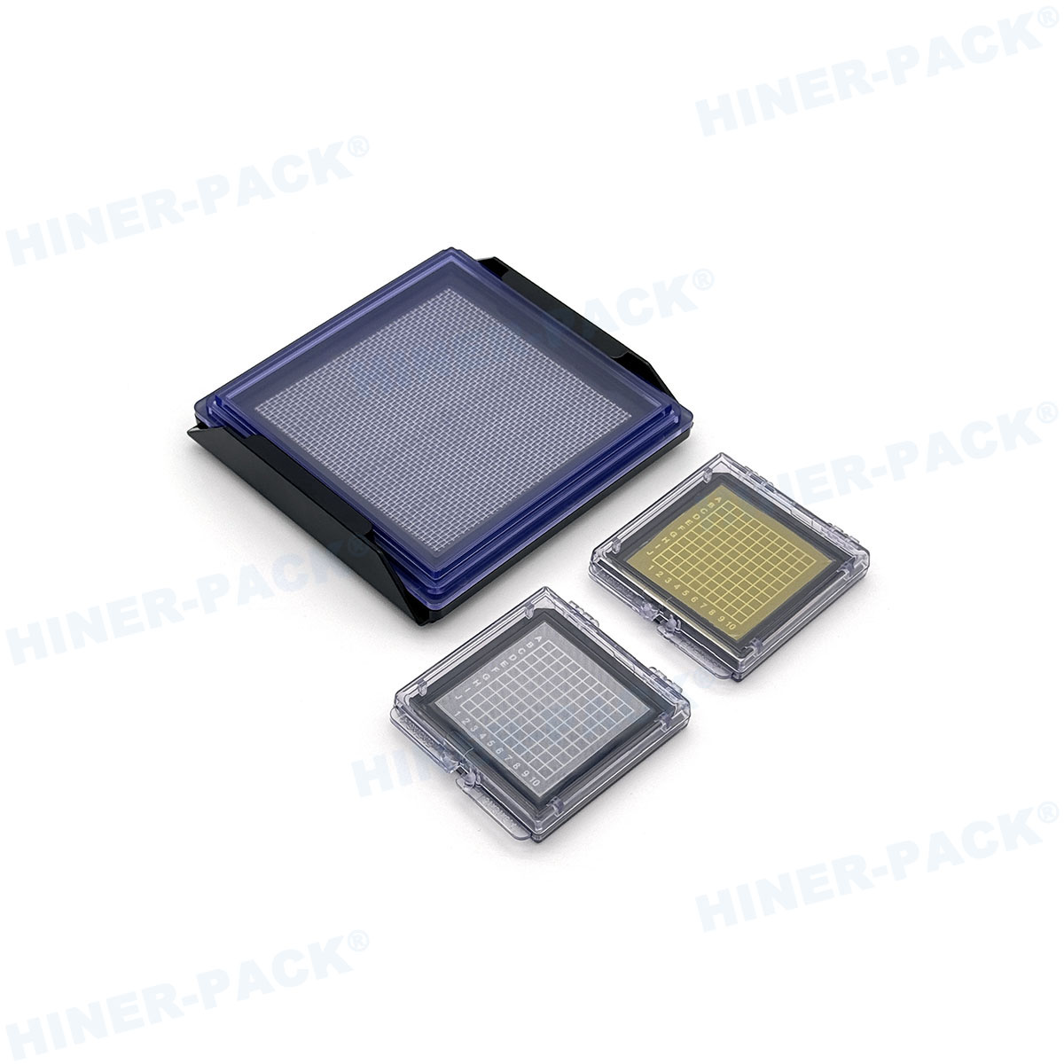
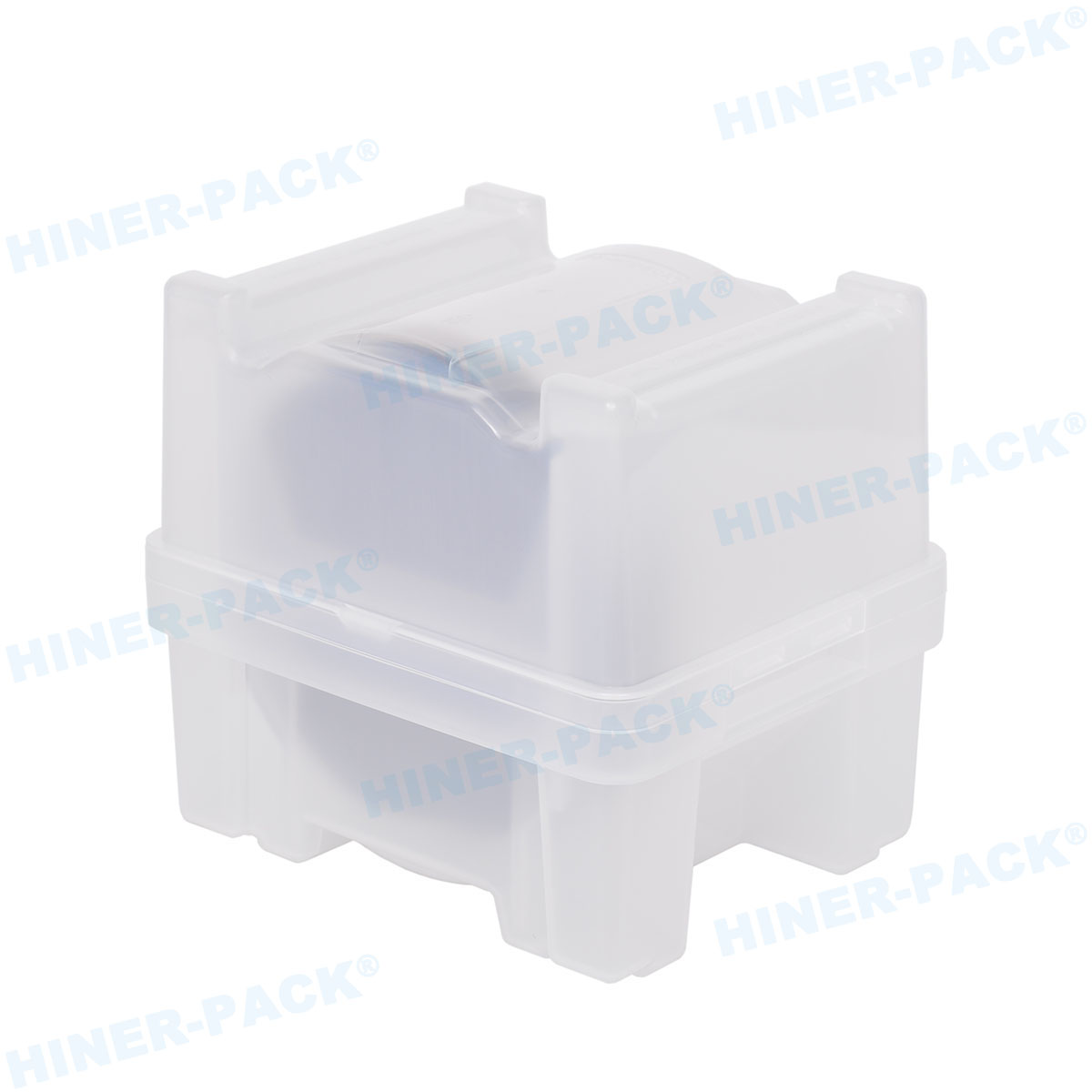
Even the most sensitive gel box electrophoresis fails if wafers are contaminated during transport or extraction. Hiner-pack provides ultra-clean wafer carriers and vacuum release boxes designed for low-particulate, low-outgassing environments. Their gel box vacuum release box (the same platform integrated into the electrophoresis workflow) ensures that wafers remain free from airborne molecular contamination (AMC) before extraction. Key features include:
Virgin polycarbonate or PFA construction with static-dissipative properties.
Vacuum-sealed lid to prevent particle ingress during storage.
Internal supports that minimize contact area to wafer edge, reducing metal abrasion.
Certified to <10 ppb extractable metals per SEMI E78-0998.
Using Hiner-pack wafer boxes in parallel with gel box electrophoresis has enabled multiple IDM fabs to achieve consistent background signals below detection limits. The synergy between clean wafer logistics and high-resolution electrophoresis is not optional – it is foundational for data integrity.
6. Optimizing Protocols for Maximum Sensitivity and Reproducibility
To push gel box electrophoresis detection limits to sub-0.5 ppb, advanced optimization is required:
Gradient gels: A 4–20% gradient gel sharpens bands for both small ions (fast migration) and larger organic complexes (slow migration) in a single run.
Two-dimensional electrophoresis: First dimension by isoelectric focusing (IEF), second by standard gel box electrophoresis. This separates contaminants by both pI and size, ideal for complex photoresist mixtures.
Stain enhancement : Use SYPRO Ruby or Flamingo fluorescent stains, which have three orders of magnitude higher sensitivity than Coomassie blue and are compatible with downstream mass spec.
Digital band quantification : Employ software with rolling ball background subtraction and lane profile deconvolution (e.g., ImageJ or GelAnalyzer). Calibrate using known standards run on the same gel.
Quality controls : Include a positive control (e.g., 1 ppb Fe-EDTA) and a negative control (extraction blank from a dummy wafer) in every gel box run.
Documentation of these parameters satisfies IATF 16949 and ISO 17025 requirements for semiconductor testing laboratories. Many foundries now include gel box electrophoresis data as a mandatory release criterion for advanced nodes (5 nm and below).
7. Comparative Analysis: Gel Box Electrophoresis vs. Alternative Techniques
To justify investment in gel box electrophoresis, it is essential to compare it with standard methods used in wafer fabs:
ICP-MS with acid digestion : Excellent total metals quantification (ppt levels) but provides no speciation, destroys the sample, and is blind to neutral organics. Gel box electrophoresis preserves sample for fraction collection and identifies charge state.
Time-of-flight SIMS : High spatial resolution but poor depth profile for soluble residues; requires ultra-high vacuum. Electrophoresis operates at ambient pressure, lower cost per sample.
Liquid particle counters : Only detect particles >20 nm, cannot identify chemical composition. Electrophoresis separates and allows chemical post-staining.
FTIR microscopy : Non-destructive but lacks sensitivity for trace metals (detection limit ~100 ppm). Not suitable for sub-ppb applications.
The unique value of gel box electrophoresis lies in its ability to bridge molecular charge and size data – two parameters that govern defect precursor activity. For R&D and failure analysis labs, the method is now considered a complementary pillar alongside ICP-MS.
8. Future Trends: Automation and Inline Coupling
The next generation of gel box electrophoresis for semiconductor fabs focuses on walkaway automation. Microfluidic gel electrophoresis chips (lab-on-a-gel) reduce reagent consumption to 2 µL per sample and cut run time to 10 minutes. Companies like Agilent and PerkinElmer have introduced prototype systems that automatically extract, load, run, and image gels. Furthermore, direct coupling of the electrophoresis output to a mass spectrometer via an electrospray interface (CE-MS) is emerging, providing real-time identification of each separated band.
Hiner-pack is actively developing wafer carriers with integrated extraction chambers, allowing seamless transfer from storage to the gel box electrophoresis sample port without human intervention – drastically reducing random handling contamination. For high-volume manufacturing, inline gel box systems that sample monitor wafers every hour are undergoing beta testing at two memory fabs. This evolution will make speciation-based contamination control a routine SPC metric.
Frequently Asked Questions (FAQ)
Q1: Can gel box electrophoresis detect neutral organic residues like
solvents or non-ionic surfactants on wafers?
A1: Standard gel box
electrophoresis separates only charged species. However, neutral residues
can be derivatized with charged tags (e.g., dansyl chloride for amines or
periodate for glycols) before electrophoresis. Alternatively, capillary
electrophoresis with indirect UV detection can be used. For routine wafer
screening, we recommend focusing on ionic residues because they cause most
electrical failures.
Q2: What detection limit can I realistically achieve for transition
metals (Fe, Cu) using gel box electrophoresis with silver
staining?
A2: With careful optimization (gradient gel, silver stain
enhancement, and background subtraction), you can reach 0.2–0.5 ppb for Fe and
Cu when extracting from a full 300 mm wafer. For lower limits, use fluorescent
stains (SYPRO Ruby) combined with laser scanning – this pushes detection to 0.05
ppb. Always validate with ICP-MS on the same extract.
Q3: How do I prevent cross-contamination between runs in the same gel
box electrophoresis cell?
A3: Implement a strict cleaning protocol:
after each run, rinse the gel tank, electrodes, and combs with 0.1 M EDTA, then
1 M HNO₃, then 18.2 MΩ·cm water. Replace running buffer every run. Use dedicated
sample loading tips. For high-sensitivity applications, dedicate a gel box cell
exclusively to wafer analysis, never for protein or DNA work. Disposable gel cassettes and
pre-cleaned accessories further reduce memory effects.
Q4: Can the same gel box electrophoresis protocol be used for both
bare silicon wafers and wafers with patterned photoresist?
A4: Yes,
but extraction conditions differ. For bare wafers, a 10-minute extraction with
0.5% HF is sufficient. For patterned wafers (photoresist present), use a 2% H₂O₂
/ 0.5% HF mixture at 40°C for 20 minutes to oxidize organic matrix and release
trapped metals. Always run a control using a wafer with known resist to ensure
no additional bands appear from resist degradation products.
Q5: What is the typical ROI for implementing gel box electrophoresis
in a 200 mm wafer fab with 10,000 wafer starts per month?
A5: Based
on three case studies, the initial capital outlay ($80k–120k for a complete
system including gel box, power supply, imager, and clean accessories) is
recouped within 8–14 months. Savings come from reduced yield loss (0.5–1.5%
improvement), fewer scrap batches due to false positives, and lower reliance on
external labs. Additionally, in-house gel box electrophoresis provides rapid feedback for cleaning bath adjustments, saving consumables.
Contact our team for a customized calculator.
Ready to integrate high-resolution gel box electrophoresis into your wafer quality program? Whether you need validated protocols, cleanroom-compatible gel boxes, or contamination-free sample handling solutions from Hiner-pack, our technical specialists are available to discuss your specific node requirements and lab setup. Request a consultation or a demo unit today – simply fill out the inquiry form below or email our semiconductor team. Every inquiry receives a detailed ROI analysis and a free test run of your wafer samples (terms apply).
Click here to submit your B2B inquiry → (Or write to sales@waferboxes.com with subject “Gel box electrophoresis for wafer analysis”). We respond within 24 hours.


