
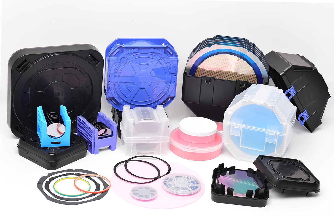
Semiconductor assembly and test operations rely on standardized carriers. The jedec tray size specification (JEDEC Standard No. 95) defines mechanical interfaces for IC shipping, baking, and automated handling. However, not all trays labeled "JEDEC" meet the same performance thresholds. Hiner-pack has supplied over 5 million injection-molded trays to OSATs (Outsourced Semiconductor Assembly and Test) and IDMs worldwide. This guide details eight verifiable parameters for procurement engineers.
1. JEDEC Tray Size Family Overview: From 2×2 to 4×8 Matrix
The JEDEC standard defines tray outer dimensions and cavity arrays. The most common jedec tray size families include:
Type I: 322mm × 135mm (12.68" × 5.31") – used for QFP, QFN, BGA up to 27×27mm body.
Type II: 322mm × 160mm (12.68" × 6.30") – wider pitch for larger ICs.
Type III: 322mm × 210mm (12.68" × 8.27") – high-density arrays for small packages (DFN, SON).
Type IV: 340mm × 250mm (13.39" × 9.84") – emerging for fan-out wafer-level packages (FOWLP).
Each family specifies cavity pitch, depth, and locating features. Mismatched trays cause jams in pick-and-place machines. Always request the exact JEDEC outline drawing (MO-###) from your supplier.
2. Dimensional Tolerances: Where Most Suppliers Fail
Even within a standard jedec tray size, critical tolerances determine automation compatibility. Inspect these three:
Overall length/width: ±0.2mm maximum. Deviations cause misfeeds in stack magazines.
Cavity pocket depth: ±0.05mm for packages ≤1.2mm thickness; ±0.08mm for thicker packages. Excessive depth allows IC tilting, leading to pick errors.
Corner radius: R1.0mm to R2.5mm as per JEDEC. Sharp corners generate particle contamination.
Hiner-pack uses coordinate measuring machines (CMM) with 1.2μm resolution to verify every mold cavity. We provide a dimensional report with each batch.
3. Material Selection: Conductive vs. Dissipative vs. High-Temperature
Semiconductor trays must control electrostatic discharge (ESD) and withstand thermal stress. The jedec tray size standard does not mandate material – but your process does. Common materials:
Polystyrene (PS) with carbon filler: Surface resistivity 10⁵–10⁹ Ω/sq. Suitable for ambient shipping and handling. Max operating temperature 70°C.
Polycarbonate (PC): Higher impact strength, withstands 120°C baking for 24 hours. Resistivity 10⁶–10¹⁰ Ω/sq.
Polyetherimide (PEI) / Ultem: Continuous use to 180°C. Used for solder reflow processes. More expensive but reusable.
PEEK (Polyether ether ketone): 260°C resistance for lead-free soldering. Rare due to cost.
For high-volume OSATs, Hiner-pack recommends conductive PC for bake-and-ship cycles. We offer custom material blends to meet specific surface resistivity (10⁴ to 10¹¹ Ω/sq).
4. Warpage Control Under Thermal and Humidity Stress
A standard jedec tray size specification assumes flatness ≤0.3mm over full length. But real-world conditions cause warpage:
After 125°C baking: PC trays may warp 0.5–0.8mm if not annealed.
After humidity absorption (85% RH, 85°C): Nylon-based trays swell, changing cavity pitch.
Solution: Request warpage data per IPC/JEDEC J-STD-020. Hiner-pack pre-conditions all trays (bake + humidity) and measures flatness on a granite surface plate. Our trays maintain ≤0.25mm warpage after 48 hours at 125°C.
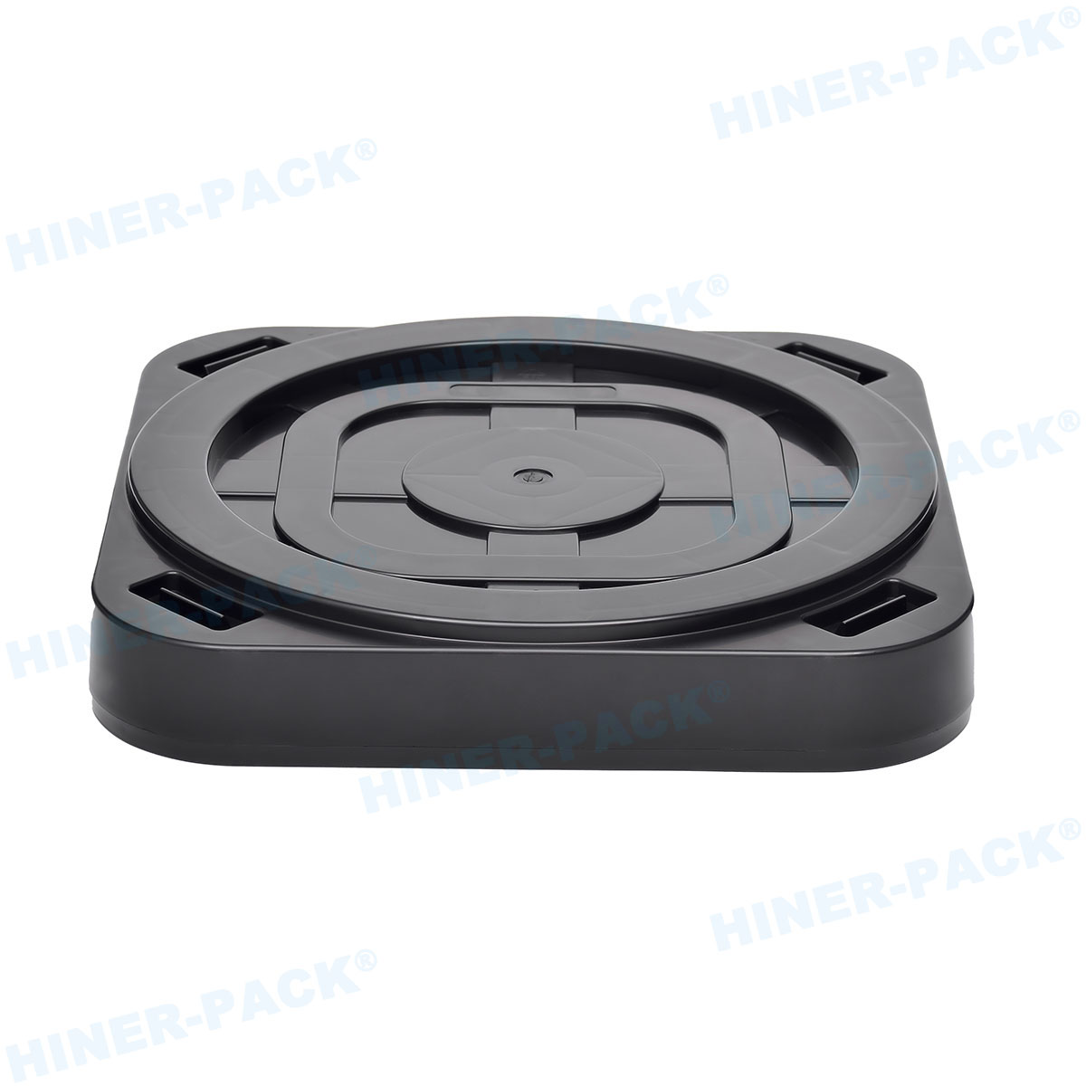
5. Stacking and Interlocking Features for Automation
Tray stacks feed automatic handlers. Poorly designed stacking ribs cause jams. Verify these features on any jedec tray size product:
Stacking ribs height: 2.0mm ±0.1mm to prevent IC-to-lid contact.
Interlocking pins and sockets: Conical design with 0.2mm clearance for self-centering.
Alignment corners: Chamfered or notched for optical sensors.
Hiner-pack's mold designs include anti-backlash stacking pins. In a recent customer test, 50,000 tray cycles showed no misfeed.
6. Cleanliness and Particle Generation Standards
Semiconductor contamination control extends to shipping trays. Requirements:
Ionic contamination: ≤0.1 µg/cm² NaCl equivalent per IEST-STD-CC1246.
Outgassing: No silicone-based mold release. Use only FDA-grade lubricants.
Particle shedding: ≤10 particles ≥0.5µm per tray after 10 minutes of vibration.
Semiconductor trays from Hiner-pack are molded in ISO Class 7 cleanrooms (Class 10,000) with ionized air rinsing. We provide a Certificate of Analysis (CoA) for each lot.
7. Common Industry Pain Points and Corrective Actions
OSAT engineers report recurring issues with jedec tray size products from low-cost suppliers. Here are three and their fixes:
Problem: ICs stick in cavities after baking. Root cause: Cavity draft angle <1°. Fix: Specify 1.5° to 2° draft and polished cavity surfaces (SPI-A2 finish).
Problem: Trays crack at stacking corners during autoclave. Root cause: Stress concentration from sharp radii. Fix: Increase corner radius to R2.0mm and use PC with 20% glass fiber.
Problem: Tray dimensions shrink after multiple reflow cycles. Root cause: Using PEI below glass transition temperature. Fix: Upgrade to PEEK or limit tray exposure to ≤5 reflow cycles.
Hiner-pack's engineering team performs failure analysis on returned trays at no charge, providing a root cause report within 10 days.
8. Why Hiner-pack Leads in JEDEC-Compliant Tray Manufacturing
With 18 injection molding presses (80 to 450 tons) and in-house tooling, Hiner-pack produces jedec tray size products that exceed standard tolerances. Our differentiators:
Tooling guarantee: All molds include replaceable cavity inserts, reducing requalification costs when IC dimensions change.
Material traceability: Lot numbers on every tray, linked to raw material certificates.
Rapid prototyping: 3D-printed sample trays in 5 days for fitment testing.
Global logistics: Warehouses in Taiwan, China, Malaysia, and Mexico with consignment stock programs.
Hiner-pack's trays are used by ASE, Amkor, and JCET for high-reliability automotive and medical ICs.
Frequently Asked Questions (FAQ)
Q1: What is the difference between JEDEC tray size Type I and Type
II?
A1: Type I outer dimensions are 322mm × 135mm; Type II is 322mm
× 160mm. Type II provides wider pitch for larger IC bodies (up to 40mm × 40mm).
Both share the same length (322mm) for compatibility with automatic magazine
loaders.
Q2: Can I use a standard JEDEC tray for ICs with exposed die or wire
bonds?
A2: No. Exposed die require anti-static cushioning or gel
trays. Standard JEDEC trays have rigid cavities that can damage wire bonds.
Hiner-pack offers custom overmolded trays with soft silicone inserts for
sensitive devices.
Q3: How do I verify if a supplier's tray meets JEDEC moisture
sensitivity level (MSL) requirements?
A3: Request MSL testing per
J-STD-020. The tray material must not absorb >0.2% moisture after 168 hours
at 85°C/85% RH. Hiner-pack provides MSL-1 certified trays for PC and PEI
materials.
Q4: What is the typical lead time for custom JEDEC tray sizes with
new cavity patterns?
A4: For a new injection mold, lead time is 6–8
weeks (including mold flow analysis and first article inspection). Hiner-pack
offers 4-week expedited service using aluminum prototype molds for up to 5,000
trays.
Q5: Are JEDEC trays recyclable after end-of-life?
A5:
Yes. PS, PC, and PEI trays are mechanically recyclable. Hiner-pack operates a
take-back program: we grind used trays into regrind and recompound into
non-critical shipping trays, reducing landfill waste by 90%.
Request a JEDEC Tray Sample Kit and Quotation
Selecting the correct jedec tray size for your IC package reduces handling damage and improves automation yield. Hiner-pack provides free sample trays (up to 50 pieces) for fitment testing on your pick-and-place equipment. We also offer dimensional inspection reports, warpage data, and material certificates.
Contact Hiner-pack’s semiconductor
division:
Website: https://www.waferboxes.com/
Email:rainbowzhu@hiner-pack.com
Phone:+86 755 2322 9236
Send your IC package dimensions (body size, thickness, pin count) and annual volume. Hiner-pack will reply with a CAD drawing, pricing, and a 3D-printed sample within 5 business days.


