In semiconductor fabs and back-end facilities, the physical and data
integrity of work-in-progress (WIP) wafers depends on a component often
overlooked: the wafer carrier
locks. These mechanisms secure front-opening unified pods (FOUPs)
and wafer shippers, preventing unauthorized access, mitigating particle
generation, and ensuring compatibility with automated material handling systems
(AMHS). This article examines the technical specifications, failure modes, and
material science behind modern locking systems—and how precision engineering
from Hiner‑pack addresses the industry's most stringent demands.
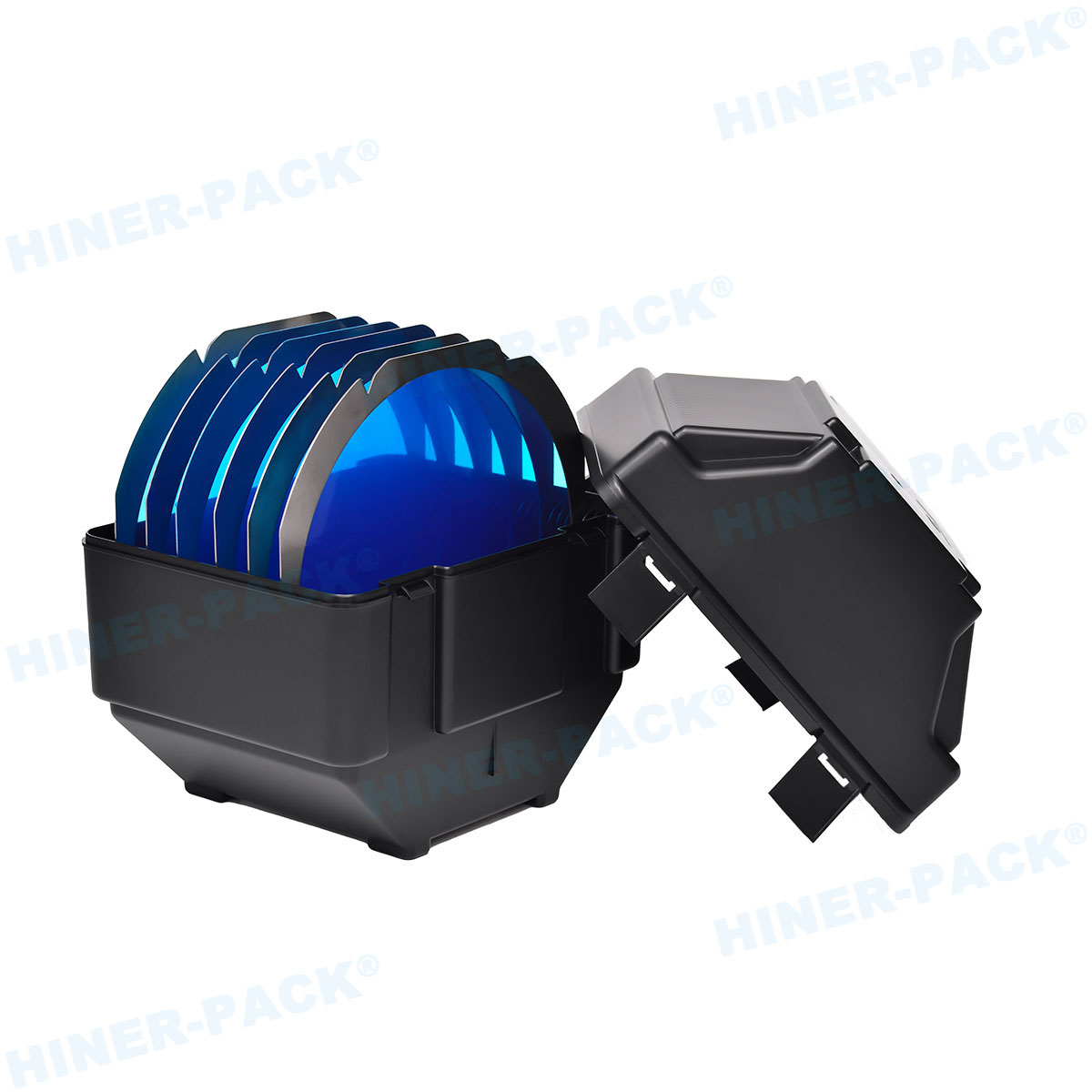
A wafer carrier lock is not a simple latch. It integrates mechanical
latching, sometimes electronic identification (RFID), and environmental sealing.
Its primary functions are:
Secure closure: Maintains a controlled micro-environment
(nitrogen purge, low humidity) during transport and storage.
Automation interface: Allows robotic load ports to
open/close the door without human intervention.
Tamper evidence: Indicates whether the pod has been opened
in uncontrolled environments.
For 300mm FOUPs, SEMI E57 and E62 standards dictate kinematic coupling and
door kinematics, but the locking mechanism's reliability directly impacts
particle counts and fab automation uptime.
Modern wafer carriers employ several locking technologies, each suited to
specific use cases—from intrabay transport to intercontinental air freight.
2.1 Mechanical Cam-Pin Locks
The most prevalent design in FOUPs uses a rotating cam that engages pins into
receiver holes in the carrier door. The cam's rotational torque must be
calibrated precisely: too low risks vibration‑induced opening; too high can
cause outgassing or particle generation from friction points. High‑performance
polymers like PEEK or statically dissipative PPS are used to minimize wear
debris.
2.2 Electronic Locks with RFID Interlock
In automated fabs, carriers are equipped with RFID tags that communicate with
the load port. Some advanced wafer carrier locks incorporate
motor‑driven latches that only open when the carrier is at the correct port and
the tag is authenticated. This prevents mis‑loading and cross‑lot contamination.
The lock actuator must consume minimal power and generate no magnetic fields
that could affect sensitive devices.
2.3 Tamper‑Evident and Security Seals
For outbound shipments, single‑use or reusable seals are integrated into the
carrier latch. These provide visual proof of integrity. Seals must withstand
harsh environmental conditions (‑40°C to 80°C) without embrittlement. Wafer carrier
locks designed for logistics often feature a dual‑stage latch: a
primary latch for automation, and a secondary manual lock for shipping.
3. Performance Requirements: Beyond Simple Closure
Selecting a wafer carrier lock requires evaluating multiple engineering
parameters. Based on 2023 industry benchmarks, the following are
non‑negotiable:
3.1 Particle Generation and Cleanliness
Any moving part generates particles. The lock mechanism must undergo rigorous
tribological testing. Industry standards require that the entire carrier
(including locks) contribute less than 0.01 particles per cubic meter per cycle
for particles >0.1µm. This is achieved through:
Contact‑less magnetic coupling (used in some high‑end designs).
Self‑lubricating bearing materials (e.g., PTFE‑filled polymers).
Hermetic sealing of the mechanism from the wafer cavity.
Hiner‑pack has
developed a proprietary low‑friction latch coating that reduces particle
shedding by over 40% compared to standard PEEK‑on‑PEEK contacts, as verified by
Fraunhofer IPA testing.
3.2 Automation Compatibility and Repeatability
A load port typically cycles a FOUP door thousands of times. The lock must
endure 10,000+ cycles without degradation in latching force or alignment.
Moreover, the force required to open the door (break‑away force) must be
consistent (±5N) to avoid robot arm faults. Precision‑molded cams and springs
from suppliers like Hiner‑pack ensure this repeatability,
directly reducing fab downtime.
3.3 Environmental Resistance and Outgassing
Carriers are subjected to nitrogen purging, vacuum bake operations, and
aggressive chemicals during cleaning. The lock materials must exhibit low
outgassing (ASTM E595: <1% TML) and withstand repeated exposure to isopropyl
alcohol or diluted HF without crazing or dimension change.
4. Industry Pain Points Related to Wafer carrier
locks Failures
Despite their small size, lock malfunctions are a leading cause of fab
interruptions. Data from major OSATs indicate:
4.1 Misalignment and Binding
If the carrier door is slightly warped (due to thermal cycling), the lock
pins can bind, causing the load port to abort the opening sequence. This results
in tool idle time and requires manual intervention—a contamination risk.
Mitigation involves stricter flatness specs for carrier doors and adjustable
latch receivers.
4.2 Spring Fatigue and Loss of Preload
The spring that maintains the lock in the closed position can relax over
time, especially at elevated temperatures (e.g., during shipping in desert
climates). A loss of preload may cause the door to vibrate open during transit,
exposing wafers to ambient air and particles. Using Inconel or coated stainless
steel springs with verified load retention is critical.
4.3 Incompatibility with Next‑Gen FOUPs
As the industry moves toward larger carriers for 450mm (though stalled) and
tighter mini‑environments, legacy lock designs may not provide adequate sealing
pressure. The lock must maintain a consistent compression of the door gasket to
keep oxygen levels below 100 ppm during nitrogen purge.
5. Solutions and Best Practices for Wafer carrier
locks Management
To mitigate these pain points, fabs and logistics providers are adopting a
holistic approach to carrier hardware.
5.1 Predictive Maintenance via Cycle Counting
Embedding RFID in the lock that tracks open/close cycles allows predictive
replacement. When a carrier approaches its end‑of‑life (e.g., 8,000 cycles), it
is pulled from circulation before failure occurs.
5.2 Material Upgrades for Low‑Particle Performance
Replacing standard acetal (POM) components with advanced tribological
compounds (e.g., Ensinger’s TECAPEEK PVX) reduces wear debris. Hiner‑pack offers a retrofit kit
for existing FOUPs that upgrades the latch mechanism to their low‑particle
design, extending carrier life by 30% while improving yield in sensitive layers
like gate oxide.
5.3 Standardization of Lock Interfaces
SEMI E111 (Mechanical Specification for FOUPs) provides guidance, but slight
variations between OEM lock suppliers can cause interoperability issues. Major
fabs now mandate that all carriers—regardless of supplier—must pass a gauge
repeatability and reproducibility (GR&R) test on a reference load port. This
drives lock manufacturers to adhere to strict tolerances.

6. Future Directions: Smart Locks and Integrated Sensors
The next generation of Wafer carrier
locks will be intelligent. Prototypes include locks with embedded
sensors for:
Real‑time humidity and oxygen measurement inside the carrier.
Shock and vibration logging during transport.
Electronic torque measurement to detect binding before it causes a
fault.
These smart locks will communicate via the carrier’s existing RFID or
Bluetooth Low Energy (BLE) tags, feeding data into the fab’s Industrial Internet
of Things (IIoT) infrastructure. For example, if a lock sensor detects excessive
vibration during truck transport, the receiving fab can quarantine that lot for
inspection.
7. The Criticality of Precision in Wafer Carrier Locks
In semiconductor manufacturing, where a single particle can cost thousands of
dollars, the humble wafer carrier
locks plays an outsized role. It ensures that the clean, controlled
environment inside the carrier is maintained from the fab to the assembly line.
As process nodes shrink and defect densities must approach zero, the engineering
of these locks will continue to evolve. Companies like Hiner‑pack are at the forefront,
providing solutions that combine mechanical robustness, material purity, and
smart technology—ultimately protecting wafer yield and enabling the economics of
advanced semiconductor production.
Frequently Asked Questions (FAQ) on Wafer Carrier Locks
Q1: What is the primary function of a wafer carrier lock beyond
keeping the door closed?
A1: Beyond physical closure, a wafer
carrier lock ensures the integrity of the internal mini‑environment by
maintaining consistent compression of the door seal. It also provides a
standardized interface for automated load ports to open and close the carrier,
and in some designs, incorporates RFID or electronic authentication to prevent
cross‑lot mixing.
Q2: How often should wafer carrier locks be inspected or
replaced?
A2: It depends on usage. In high‑volume fabs where
carriers cycle multiple times daily, inspection every 3‑6 months is recommended.
Look for signs of wear such as inconsistent latching force, visible debris, or
increased particle counts in the carrier. Many fabs implement a preventive
maintenance schedule based on cycle count (e.g., every 5,000 cycles) rather than
time.
Q3: Can a worn wafer carrier lock increase particle
contamination?
A3: Yes. As lock components wear—particularly the cam
and pin interfaces—they generate microscopic particles. These particles can
migrate into the wafer storage area if the lock is not sealed from the interior.
Additionally, a worn lock may not seal the door properly, allowing external
particles to enter. Using low‑wear materials from suppliers like Hiner‑pack is essential for
particle control.
Q4: Are wafer carrier locks standardized across all FOUP
brands?
A4: While SEMI standards (e.g., E57, E62) define the overall
geometry and kinematic coupling, the exact locking mechanism design can vary
between manufacturers. This can lead to interoperability issues with certain
load ports. To mitigate this, many semiconductor companies qualify carriers from
multiple vendors but require that the lock mechanisms meet specific force and
cycle life criteria defined in their internal specifications.
Q5: What materials are best for minimizing outgassing in wafer
carrier locks?
A5: For critical applications, especially those
involving vacuum or sensitive deposition processes, materials with very low
total mass loss (TML) are required. Polyetheretherketone (PEEK) and certain
grades of polyamide‑imide (PAI) are commonly used. Metallic components should be
coated or passivated to prevent oxidation. Wafer carrier
locks from premium suppliers often come with certification of
outgassing test results per ASTM E595.
Q6: How do smart wafer carrier locks interface with factory
automation systems?
A6: Smart locks typically integrate with the
carrier’s existing RFID or add a dedicated sensor module. Data such as latch
position, cycle count, or internal environment parameters are transmitted
wirelessly to the material control system (MCS). This allows the fab to track
carrier health in real time and preemptively remove problematic carriers from
the automated handling system.


