1. The Uncompromising Demands of Modern Wafer Transport
Today’s semiconductor ecosystem operates across global supply chains. Wafers—ranging from 150mm legacy to 300mm and emerging 200mm SiC substrates—must traverse continents while maintaining cleanliness levels compatible with ISO Class 4 (formerly Class 10) cleanrooms. Generic, one-size-fits-all carriers often fall short. Key technical stressors include:
Particle contamination: Even sub-0.1µm particles can create killer defects in 5nm node devices.
ESD vulnerability: Thin gate oxides are susceptible to discharges as low as 50V.
Mechanical strain: Vibration during air/road freight induces micro-cracks at wafer edges.
Moisture & outgassing: Certain polymers release volatiles that cause haze or corrosion.
Addressing these requires a departure from off-the-shelf trays. True custom wafer shippers integrate application-specific geometry, material blends, and supplementary accessories such as conductive foam inserts or humidity buffers. A study by the International Semiconductor Manufacturing Technology consortium noted that facilities deploying purpose-built wafer shippers reduced in-transit defectivity by 37% compared to generic alternatives.
2. Core Technologies Behind High-Performance Custom Wafer Shippers
2.1 Substrate-Specific Material Selection
Not all polymers are equal. For advanced nodes, the industry favors carbon-loaded polypropylene (PP) or polycarbonate (PC) blends with surface resistivity between 10³ – 10⁵ Ω/sq to provide static dissipative properties without sparking. For extreme low-outgassing requirements (e.g., EUV mask shipping), perfluoroalkoxy (PFA) coatings are sometimes applied. Hiner-pack employs compounding techniques that tailor conductivity, stiffness, and chemical purity, ensuring that each custom wafer shipper meets SEMI E89 (ESD) and SEMI E151 (fluids compatibility) guidelines.
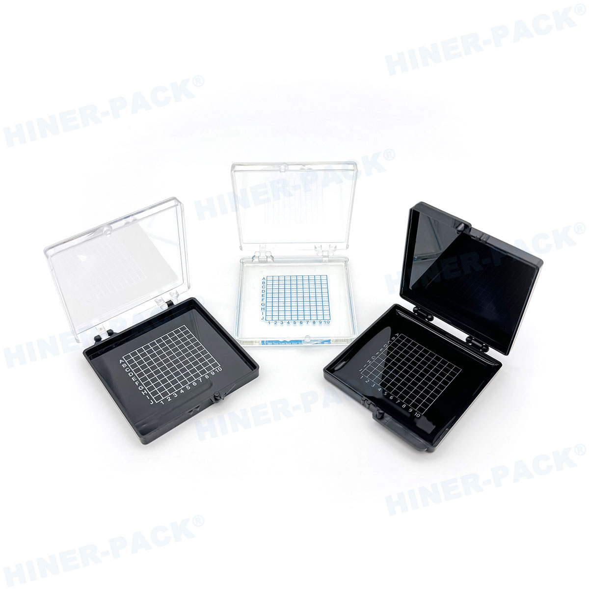
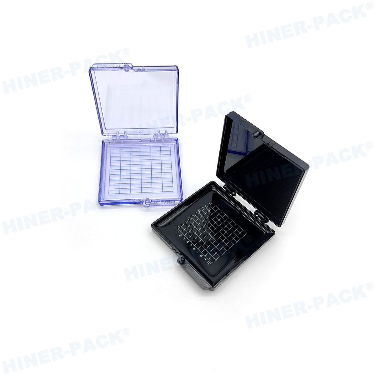
2.2 Precision Pocket Design & Edge Support
Wafers are typically supported at the bevel or via multiple contact points. Finite element analysis (FEA) is employed to simulate stacking loads, vibration resonance, and insertion/withdrawal forces. For 300mm wafers, advanced shippers use “contactless” retention—a kinematic mount that immobilizes the wafer without touching the device area. This is critical for bumped wafers or micro-electromechanical systems (MEMS). Custom pocket geometries also accommodate wafer bow (up to 3mm for some SiC substrates) without inducing stress.
2.3 Modular Accessories and Identification Systems
Beyond the base tray, modern custom wafer shippers incorporate:
Conductive silicone or polyurethane gaskets for vibration dampening.
RFID tags and barcode wells for automated lot tracking (SECS/GEM compliance).
Custom-fit desiccant compartments for moisture-sensitive devices.
Interlocking stack ribs to prevent collapse during palletization.
Such accessories are often manufactured in parallel with the main shipper to ensure perfect fit and consistent performance. Comprehensive accessory portfolios are available via dedicated wafer shipper accessory lines that complement the primary custom design.
3. Industry-Specific Application Scenarios
The concept of custom wafer shippers extends across several semiconductor verticals, each with unique pain points:
Advanced Logic (7nm/5nm/3nm): Ultra-low particle generation, extreme flatness requirements, and ESD protection with surface resistivity tightly controlled. Shippers often include 100% inspection of inner surfaces via laser particle counters.
Power Devices (SiC, GaN): Wafers with larger bow/warp require adjustable or custom-molded support pockets; thermal management considerations for high-temperature pre-shipping processes.
MEMS & Sensors: Fragile membrane structures mandate minimal acceleration transfer. Custom shippers integrate vibration-damping foam inserts calibrated to ISO 13355 random vibration profiles.
Photomasks & Reticles: While not traditional wafers, similar principles apply: custom shipping solutions for pellicle-protected masks require zero-contact handling and ultra-clean polymers.
Each scenario demands that the shipper designer collaborates early with process engineers. Hiner-pack employs a consultative engineering workflow—including 3D scanning of existing automation equipment (EFEMs, sorter tools) to guarantee that custom wafer shippers align with robotic end-effectors and industry-standard FOUP-like interfaces.
4. Technical Validation: How Custom Designs Are Qualified
Before deployment, rigorous testing protocols validate the performance of any custom wafer shipper. Leading OEMs and wafer manufacturers mandate:
ISTA 3A / ASTM D4169: Simulated distribution testing with vibration, drop, and compression profiles tailored to air/ground transport.
SEMI E10 / E15: Cleanliness characterization – liquid particle count (LPC) and non-volatile residue (NVR) analysis to ensure outgassing remains below <0.05 µg/cm².
ESD TR53 / ANSI/ESD STM11.11: Surface resistivity and charge decay time verification.
Accelerated aging: Exposure to temperature cycling (-40°C to 70°C) and UV radiation to simulate global logistics.
Only after passing these thresholds does a custom design enter production. Hiner-pack maintains ISO 9001:2015 and ISO 14644-1 Class 7 cleanroom manufacturing, ensuring that every batch of custom wafer shippers is produced under 1,000-class conditions with continuous SPC monitoring.
5. Economic Impact: Beyond Protection to Cost Optimization
While the upfront investment in custom wafer shippers is higher than standard foam-lined boxes, the total cost of ownership (TCO) analysis reveals compelling advantages:
Yield preservation: Reducing defect density by 0.05% for a high-volume 300mm fab translates to annual savings of $2M–$5M.
Reusability cycles: Precision injection-molded shippers often sustain 100+ wash cycles without performance degradation, whereas generic carriers show wear after 20 cycles.
Automation compatibility: Custom-designed dimensional accuracy prevents tool jams, reducing downtime by up to 15% in automated material handling systems (AMHS).
Inventory reduction: A single custom design that accommodates multiple wafer types (e.g., 200mm epi and monitor wafers) reduces SKU complexity.
Leading IDMs report that transitioning to fully customized wafer shipping solutions shortened their logistics cycle times by 22% and eliminated a major recurring source of excursion events.
6. Future Trends: Intelligent and Sustainable Custom Wafer Shippers
As Industry 4.0 permeates semiconductor logistics, custom wafer shippers are becoming smarter. Embedded IoT sensors now track shock, humidity, and temperature in real-time, transmitting data to cloud-based platforms for predictive maintenance. Moreover, sustainability mandates drive material innovation: recycled engineering plastics, bio-based polymers, and design-for-disassembly concepts are gaining traction. Hiner-pack has pioneered a closed-loop recycling program for used wafer shippers, reprocessing materials into new shipping components without compromising cleanliness or mechanical properties.
Another frontier is the convergence of custom shippers with wafer-level packaging (WLP) handling. As fan-out and 3D-IC technologies require thin-wafer support during shipment, custom shippers are evolving to incorporate temporary bonding frames and protective adhesive layers directly into the carrier architecture.
7. Why Engineering Partnership Matters
The difference between a satisfactory shipper and a truly optimized one lies in the depth of collaboration. Hiner-pack integrates design, prototyping, and validation under one roof, offering:
CAD-based pocket optimization and rapid tooling (3–5 weeks for first articles).
On-site contamination analysis via SEM/EDX and FTIR to verify material purity.
Custom accessory integration—from ESD foams to RFID tags—ensuring full system compatibility.
Documentation packages including certificate of conformance, validation reports, and SEMI compliance certificates.
By treating each project as a mission-critical development rather than a procurement item, Hiner-pack helps customers achieve lower variance in transit defect rates and higher throughput for global wafer logistics.
Precision Is Not Optional
In the semiconductor industry, margins are measured in angstroms and parts-per-billion. Off-the-shelf packaging introduces unnecessary variables. Transitioning to purpose-built custom wafer shippers aligns logistics with the same discipline as wafer processing: controlled, validated, and continuously improved. For facilities seeking to protect high-ASP substrates and maximize operational efficiency, the shift to engineered, application-specific wafer carriers is no longer a luxury—it’s a competitive imperative.
Frequently Asked Questions (FAQ)
Q1: What are the primary differences between standard wafer shippers and custom wafer shippers?
Standard wafer shippers are mass-produced with generic pocket dimensions, often supporting only basic wafer sizes (e.g., 200mm) with limited material choices. Custom wafer shippers, in contrast, are engineered to match specific wafer geometries (including warped or thin wafers), incorporate optimized ESD properties for sensitive devices, and may integrate automation alignment features. They also undergo application-specific validation such as vibration profiling tailored to a client's logistics chain, resulting in significantly lower defect rates.
Q2: Which materials are typically used for custom wafer shippers in advanced node fabs (sub-10nm)?
For sub-10nm nodes, materials must exhibit ultra-low outgassing, low extractable metals, and precise surface resistivity. The most common are carbon-fiber reinforced polycarbonate (PC) or polypropylene (PP) blends with surface resistivity controlled between 10³ and 10⁵ Ω/sq. Some designs employ a co-molded construction with a conductive core and a virgin contact layer to minimize particle generation. Hiner-pack also offers PFA-coated variants for EUVL mask shipping where volatile condensables are strictly prohibited.
Q3: How are custom wafer shippers validated for cleanroom compatibility?
Validation includes SEMI E10 cleanliness tests: liquid particle count (LPC) to quantify detachable particles >0.1µm, non-volatile residue (NVR) extraction, and ionic contamination analysis per SEMI E45. In addition, custom designs are often tested in actual cleanroom environments using automated material handling systems (AMHS) to confirm compatibility with load ports and robotic end-effectors. Manufacturers like Hiner-pack provide a full validation package documenting these metrics for each production lot.
Q4: Can custom wafer shippers be designed to accommodate both 150mm and 200mm wafers in a single carrier?
Yes, through modular insert designs or stepped pocket geometries, it is possible to create a universal platform that securely holds multiple wafer sizes. However, careful FEA analysis is required to ensure the insert does not introduce particle generation points. Custom wafer shippers with exchangeable trays allow a single external case to accommodate different wafer diameters, reducing SKU count and simplifying logistics for mixed-node fabs.
Q5: What is the typical lead time for developing a new custom wafer shipper from concept to production?
Depending on complexity and the need for tooling, the timeline ranges from 6 to 12 weeks. The process includes initial design review (1–2 weeks), prototype tooling and sampling (3–4 weeks), validation testing (2 weeks), and production tooling ramp (2–4 weeks). Hiner-pack utilizes in-house mold-making and cleanroom molding to expedite this timeline while maintaining full traceability and compliance with SEMI standards.
Q6: Are there cost-effective options for low-volume or R&D wafer shipper needs?
Absolutely. For pilot lines or R&D facilities, Hiner-pack offers small-batch production using aluminum or rapid tooling, as well as semi-custom designs derived from existing modular platforms. This approach provides many benefits of customization—such as precise pocket geometry and ESD control—without the full investment of high-volume injection molds, making custom wafer shippers accessible for prototyping and early-stage production.
For further technical consultation or to discuss a specific wafer shipping challenge, visit Hiner-pack to explore engineering resources and application support.