For semiconductor engineers handling bare die, micro-electromechanical
systems (MEMS), or small-lot specialty ICs, the choice of shipping and
processing carrier directly influences yield and long-term reliability. The
antistatic waffle
pack chip tray has emerged as the preferred solution for
applications requiring individual die isolation, static dissipation, and
compatibility with automated pick-and-place equipment. Unlike matrix trays
designed for high-volume JEDEC packages, waffle pack trays feature a unique grid
of individual pockets (often 2×2 inch or 4×4 inch footprints) that hold single
chips, preventing die-to-die contact and mechanical abrasion. This article
provides a technical analysis of materials, ESD performance, industry pain
points, and selection criteria for antistatic waffle
pack chip trays, drawing on two decades of engineering data from
tier-1 OSATs and fabless semiconductor houses. Hiner-pack offers a
comprehensive portfolio of these trays, designed for cleanroom use, temperature
cycling, and high-vibration logistics.
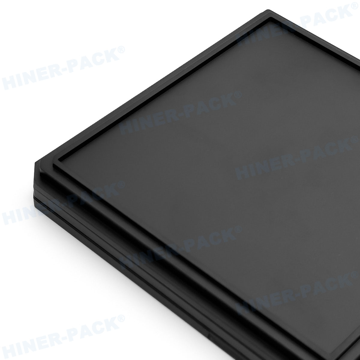
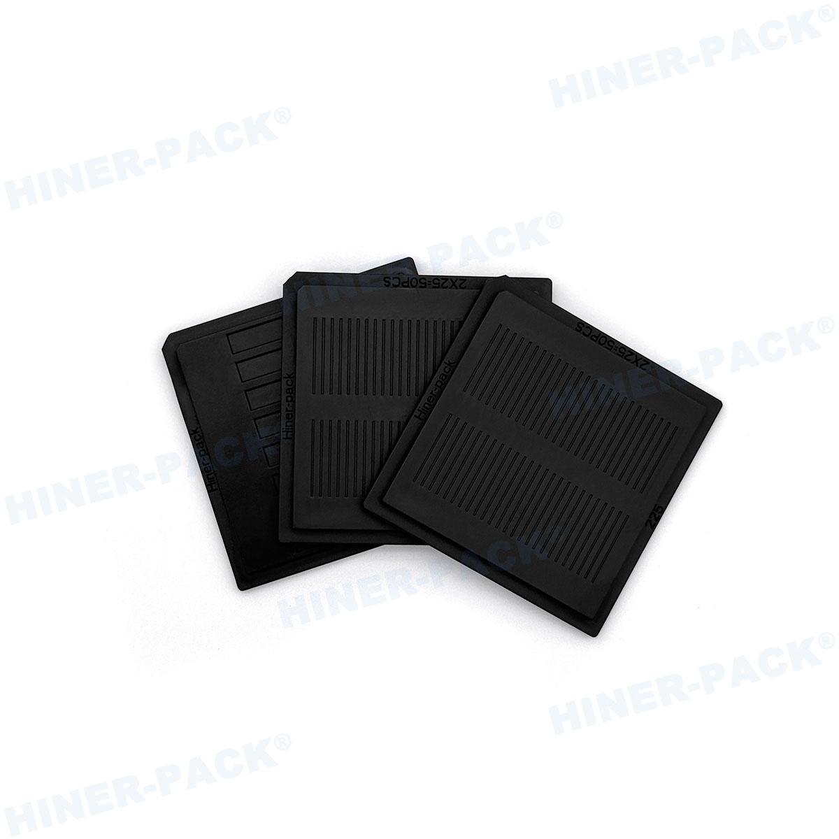
1. What Defines an Antistatic Waffle Pack Chip Tray?
The term "waffle pack" describes the raised pocket walls that form a
waffle-like pattern across the tray surface. Each pocket precisely matches the
dimensions of a specific die size (e.g., 3×3 mm, 5×5 mm, 10×10 mm). The
"antistatic" property refers to surface resistivity typically in the
static-dissipative range (106 to 109 ohms/square), which
prevents triboelectric charging during sliding or vibration. Key characteristics
of a genuine antistatic waffle
pack chip tray include:
Individual cavity array: Usually 8×12, 10×14, or 12×18
pockets per tray, depending on die dimensions.
Static-dissipative polymer: Carbon-loaded polyethylene
terephthalate (PET), polycarbonate (PC), or polyethersulfone (PES).
Lid compatibility: Designed to accept a conductive or
antistatic lid (tape or rigid cover) for stacking and shipping.
Smooth cavity floor: Minimum surface roughness (Ra ≤ 0.4
µm) to prevent scratching of die backside.Compared to gel packs or standard shipping tubes, the antistatic waffle
pack chip tray offers superior mechanical isolation and ESD
protection, especially for high-value devices such as GaN-on-Si dies, SAW
filters, and optical sensors.
2. Technical Deep Dive: Materials, Resistivity, and Environmental
Limits
Selecting an antistatic waffle
pack chip tray requires evaluating four interdependent parameters:
surface resistivity, thermal range, outgassing profile, and pocket dimensional
accuracy. Below are the industry benchmark specifications for each material
class, with Hiner-pack’s engineering recommendations.
2.1 Surface Resistivity & ESD Class
Static-dissipative (preferred): 1×10⁶ Ω/sq to
1×10⁹ Ω/sq – sufficient for devices with HBM sensitivity >250V.
Decay time <0.5 seconds per ANSI/ESD STM11.11.
Conductive (optional): 1×10³ Ω/sq to
1×10⁵ Ω/sq – for extremely sensitive devices (<100V HBM). But risk
of micro-shorting if die contacts exposed metal to tray.
Volume resistivity: >103 Ω·cm to avoid
leakage path through the tray thickness.
2.2 Thermal & Mechanical Performance
Operating temperature: -40°C to +85°C for standard PC-based
trays; extended range -40°C to +160°C for PES or PEI (polyetherimide)
materials.
Warpage limit: ≤0.15 mm over 100 mm length after 24 hours
at 85°C/85% RH (per JEDEC JESD22-B112).
Pocket depth tolerance: ±0.025 mm to ensure die does not
protrude above cavity rim, preventing lid damage.
Flexural modulus: 2,500–4,500 MPa for automated die
ejectors.
2.3 Material Selection Guide
Hiner-pack offers three families
of antistatic waffle pack materials, each aligned with specific semiconductor
back-end processes:
| Base Resin | Antistatic Additive | Resistivity (Ω/sq) | Max Temp | Best suited for |
|---|
| Polycarbonate (PC) – clear | Internal permanent antistatic (IPAS) | 107–109 | 85°C | Visual inspection, pick-and-place, short-term storage |
| Polyethersulfone (PES) | Carbon fiber 10% | 106–108 | 160°C | Bake-out, die attach prep, high-temp logistics |
| Polycarbonate (PC) – black conductive | Carbon black 15-20% | 104–106 | 85°C | High-sensitivity GaAs, InP, RF dies |
Each material passes outgassing tests per SEMI F57 (for cleanroom compatibility), with total mass loss <0.5% and
collected volatile condensables <0.1%. Hiner-pack provides a material
declaration and ionic cleanliness report for every lot.
3. Industry Pain Points and Engineered Solutions
Semiconductor assembly and test facilities regularly encounter four critical
problems that directly affect die yield. Below is how a properly specified
antistatic waffle
pack chip tray resolves each issue:
3.1 ESD-induced die damage during manual handling
Non-antistatic trays (insulative plastics >1012 Ω/sq) generate
charges up to 15 kV from friction with ESD garments or gloves. Dissipative
waffle pack trays keep charge below 50V, completely preventing gate oxide
breakdown. Hiner-pack trays incorporate internal antistatic agents that remain
functional after >500 washing cycles.
3.2 Die chipping from pocket movement
Improper pocket geometry (excessive clearance) allows the die to slide and
strike pocket walls, causing edge chipping. Our waffle pack trays use precision cavity
design with a clearance of only 0.1 mm to 0.2 mm per side,
preventing lateral movement while allowing automated vacuum pickup. Each cavity
includes a 0.05 mm chamfer at the entry to guide the die during manual placement
without stubbing.
3.3 Particle contamination from tray abrasion
Conventional black carbon-loaded trays shed conductive particles (carbon
agglomerates) that short bond pads or create leakage paths. Hiner-pack uses
anti-dust carbon fiber or inherently dissipative polymers (IDP) to eliminate
particle shedding. Particle count per tray is controlled to <200 particles
>0.3 µm, validated by liquid particle counter (LPC) per ISO 14644-10.
3.4 Incompatibility with automated die sorters
Many waffle pack trays lack registration holes or edge rails, causing
misfeeds in machines like the Mühlbauer MSL91 or Data IO. Hiner-pack
incorporates SEMI-compliant 3 mm index holes and corner notches, fully
compatible with standard JEDEC tray handling systems. Our design guide details
pocket pitch that matches common pick-and-place nozzle grids (e.g., 4 mm, 8 mm,
12 mm).
4. Application Scenarios Across the Semiconductor Value Chain
Antistatic waffle
pack chip trays are deployed in five distinct stages where low
volume but high die value necessitates individual isolation:
Wafer sawing and die sorting: After dicing, known good die
(KGD) are placed into waffle pack trays by automatic die sorters. Trays need
high flatness to avoid die tilt during vision inspection.
Hybrid assembly (MCM, SiP): Multiple different die types
(controller, memory, passives) are kitted from waffle trays onto substrate
attach machines. Color-coded or engraved tray identification prevents
mix-ups.
Failure analysis (FA) lab: Faulty dies are transported to
FA for SEM/EDX analysis. Antistatic protection is mandatory to avoid additional
ESD artifacts. Clear PC trays allow optical inspection without opening.
Prototyping and engineering builds: For new products
requiring small quantities (50–500 units), waffle pack trays offer economical
reusability compared to tape-and-reel.
Military/aerospace die banking: Long-term storage (≥5
years) of radiation-hardened or high-reliability dies. Trays must pass
accelerated aging per Mil-STD-883, method 1010.
In all these scenarios, the antistatic waffle
pack chip tray outperforms gel packs (which dry out) and Matrix
trays (which are overkill for low quantities). The average cost-per-use drops
below $0.001 per die after 20 reuses.
5. Hiner-pack’s Differentiated Engineering for Waffle Pack Trays
While several vendors offer generic antistatic trays, Hiner-pack has developed four
proprietary enhancements specific to waffle pack platforms:
Cavity-specific laser marking: Each pocket can be engraved
with a unique 2D Data Matrix code for full traceability at the individual die
level – critical for automotive PPAP and medical device regulations.
Custom stack keys and nesting ribs: Prevents tray inversion
and mis-stacking that can crush dies. Stacking height tolerance is ±0.05 mm for
seamless magazine loading.
Built-in ESD grounding tabs: Metal contact points on the
tray edge allow automatic discharge when the tray enters an equipment loader,
eliminating charge accumulation during conveyance.
Low-profile pocket walls (2.0 mm vs standard 3.5 mm): Reduces overall stack height by 30%, increasing shipping density while
maintaining die protection. Validated via JEDEC vibration and drop
tests.
All Hiner-pack waffle pack trays comply with SEMI
E15.93 (carrier dimensional standard) and are manufactured in an
ISO Class 7 cleanroom with 100% automated optical inspection (AOI) of each
cavity for flash or damage.
6. Best Practices for Cleaning, Handling, and Reuse
To maximize lifetime value of your antistatic waffle
pack chip tray, implement the following operational protocols
recommended by Hiner-pack’s process engineering team:
Initial cleaning: New trays should be rinsed with deionized
water and dried in a laminar flow hood (no heat >60°C). Avoid air guns that
may cause electrostatic charge.
Post-use cleaning: Ultrasonic bath (40 kHz) in 2% alkaline
detergent for 5 minutes, followed by three DI water rinses. Do not use abrasive
brushes that may modify surface resistivity.
Drying: Forced air drying at 50°C for 2 hours. Verify
surface resistivity after every 25 cleaning cycles using a concentric ring probe
(per ANSI/ESD STM11.11).
Storage: Stack trays with protective cardboard sheets
between each unit; store at 20-25°C, 40-60% RH. Avoid UV exposure to prevent
polymer degradation.
Retirement criteria: Replace trays when warpage >0.2 mm
over 100 mm or resistivity drifts outside specification range. Hiner-pack offers
a trade-in program for end-of-life trays.
Following these steps typically extends tray service life to 500-800 cycles,
reducing cost of ownership by 40% compared to single-use alternatives.
7. Global Standards and Certification
Procurement and quality engineers must verify that antistatic waffle
pack chip trays meet the following normative references:
ANSI/ESD S20.20-2021: Corporate ESD program compliance
(tray as process essential insulator).
JEDEC JESD625-B: Requirements for handling ESD-sensitive
devices.
SEMI E10-0304: Specification for shipping carriers of die
and wafers.
IPC/JEDEC J-STD-033D: Handling of moisture-sensitive
components (MSL level 2a or higher).
Mil‑STD‑750-5: High-temperature storage life for military
applications.
Hiner-pack provides a
comprehensive certificate of compliance (CoC) with each shipment, including
lot-specific resistivity measurements, flatness data, and outgassing
chromatograms. Full material disclosure (complete ELV and REACH declarations) is
available upon request.
8. Future Trends: Smart Waffle Pack Trays and AI-Driven Die Kitting
The next generation of antistatic waffle
pack chip trays is moving toward embedded RFID and thin-film
humidity sensors. Hiner-pack is developing in-mold label electronics
(IMLE) that record tray environmental history (temperature spikes,
moisture exposure) without compromising ESD properties. These data are read by
automated warehouse systems to route trays to appropriate drying ovens before
use. Additionally, AI vision systems now recognize die positions within waffle
trays to optimize pick sequence, reducing pick errors by 60% in prototype
assembly lines. Early adopters report 22% reduction in mis-picks and 30% faster
changeover times.
Frequently Asked Questions (FAQs)
Q1: What is the difference between an antistatic waffle pack tray and a
JEDEC matrix tray?
A1: A waffle pack tray features individual pockets in a
low-density grid (typically <200 pockets) and is designed for bare die, small
ICs, or mixed part numbers. A JEDEC matrix tray has high-density pockets (up to
1200 cavities) conforming to specific package outlines (e.g., TQFP, BGA) and is
intended for large-volume surface-mount assembly. Waffle packs offer more
flexibility for die sizes but lower throughput per tray.
Q2: Can antistatic waffle pack chip trays be used for moisture-sensitive
devices (MSL)?
A2: Yes, but with precautions. Trays alone do not provide a
moisture barrier. For MSL devices, the waffle pack tray must be sealed inside a
moisture barrier bag (MBB) with desiccant and a humidity indicator card (HIC).
Hiner-pack offers tray-lid assemblies with integrated foil sealing film,
compatible with vacuum packing per J-STD-033. For MSL level 3 or below, dry
packing is mandatory.
Q3: How do I measure the surface resistivity of a used waffle pack
tray?
A3: Use a concentric ring probe (e.g., ACL 800 or Prostat
PRS-801) connected to a megohmmeter. Apply 100V test voltage, place the probe on
a flat area (not inside a cavity). Measure five points per tray and average the
values. Resistivity should remain within ±0.5 decade of the original
specification. Clean trays before testing to remove contamination.
Q4: Are there antistatic waffle pack trays that withstand soldering reflow
temperatures (peak 260°C)?
A4: No standard polymer tray can withstand reflow. For
in-process applications requiring reflow compatibility, you need a metal or
ceramic carrier. However, Hiner-pack offers polyetherimide (PEI) waffle trays
with service up to 180°C for bake-out before encapsulation. For any process
above 180°C, transfer parts to a dedicated reflow carrier.
Q5: Can I get custom cavity shapes for non-rectangular dies (e.g., GaAs
power amplifiers with odd footprints)?
A5: Yes. Hiner-pack provides custom injection molding for
any cavity geometry – including stepped pockets, corner radius, or angled side
walls. Minimum tooling lead time is 4 weeks for prototype quantities (50-100
trays). The cavity is machined using CNC graphite electrodes for tight tolerance
(≤±0.015 mm). Request a design review with our engineering team for complex
shapes.
Q6: How do antistatic waffle pack trays perform in automated die sorters
like the NeuTek NT2000?
A6: The tray must have precise registration holes (2-2.5 mm
diameter, 3 mm from edge) and a flatness under 0.15 mm across the pick area.
Hiner-pack trays are tested on NeuTek, Mühlbauer, and Fasford equipment. We
supply a compatibility matrix and recommend a trial run with 10 sample trays
before full deployment. Most pick-and-place errors arise from tray warpage – our
annealing process eliminates this.
Request a Technical Quotation & Engineering Sample
Selecting the correct antistatic waffle
pack chip tray requires evaluating die dimensions, ESD sensitivity,
thermal exposure, and automation equipment. Hiner-pack offers free sample
trays (up to 10 units) for on-site validation. We provide a complete technical
data sheet including cavity drawings, material certs, and ESD test reports. For
custom designs, submit your die outline drawing and annual volume. Our team
responds with a preliminary stack-up design within 48 hours.
Send your inquiry to Hiner-pack’s semiconductor packaging
division using the contact form at https://www.waferboxes.com/ or
email directly to rainbowzhu@hiner-pack.com. Include your target pocket array, die
size tolerance, and any cleanroom class requirement. We will provide a
commercial proposal, lead time, and a sample kit for first-article inspection.
For urgent prototyping (less than 3 weeks), expedited tooling service is
available.