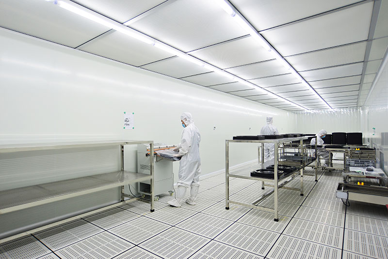
In advanced semiconductor manufacturing, test, and surface-mount assembly,
the physical carrier protecting sensitive devices is as critical as the process
itself. Conductive JEDEC
matrix IC trays have become the non-negotiable standard for
handling high-density packages such as BGAs, QFNs, CSPs, and FCs. These trays
combine precise cavity geometry, static-dissipative or conductive polymers, and
strict compliance with JEDEC publication 95 (and related outlines) to prevent
electrostatic discharge (ESD) damage, mechanical stress, and contamination. For
over a decade, Hiner-pack has engineered these
trays for tier-1 OSATs, fabs, and automotive IC suppliers, integrating
carbon-fiber or inherently conductive compounds with matrix architectures that
maximize throughput in automated handlers. This article dissects the material
science, industry pain points, compliance frameworks, and selection criteria for
conductive JEDEC
matrix IC trays, offering actionable guidance for procurement and
process engineers.
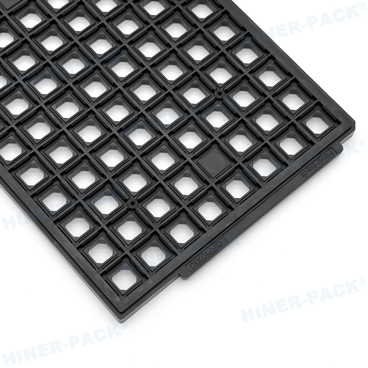
1. What Defines a Conductive JEDEC Matrix IC Tray?
A JEDEC matrix tray is a rigid, injection-molded carrier
that organizes hundreds of individual ICs in a grid (rows and columns) while
conforming to dimensional standards set by JEDEC Solid State Technology
Association. The terms "conductive" refers to surface resistivity ≤
105 ohms/sq (often 103–105 Ω/sq), enabling
rapid charge dissipation to ground. Key differentiators include:
Matrix configuration: Fixed cavity pockets arranged in X-Y
arrays (e.g., 20×30, 16×40) for robotic pick-and-place alignment.
JEDEC compliance: Meets or exceeds outlines such as MS-001,
MS-026, MO-019 for tray coplanarity, thickness, and corner radius.
Conductive loading: Carbon black, carbon fiber, or
inherently dissipative polymers (IDPs) blended into base resins (PC, PES, PPS,
PEI).
ESD performance: Static decay rate <0.5 seconds and
shielding from triboelectric charging.
The conductive JEDEC
matrix IC trays from Hiner-pack are validated to
ANSI/ESD S20.20 and S11.11, offering consistent surface resistivity across
temperature cycling (-40°C to 125°C) and humidity variations. Unlike coated
trays (which delaminate), our conductive compounds provide permanent ESD
protection without outgassing or particle shedding — critical for Class 10
cleanrooms.
2. Technical Specifications & Material Science Deep Dive
Selecting conductive JEDEC
matrix IC trays requires evaluating four interdependent parameters:
electrical properties, thermal stability, mechanical rigidity, and chemical
resistance. Below are industry benchmark metrics and ESD-safe materials commonly adopted:
2.1 Surface Resistivity & ESD Class
Conductive range: 1×10³ Ω/sq to 1×10⁵ Ω/sq – ideal for devices sensitive to <100V HBM (human body model).
Static-dissipative range: 1×10⁶ Ω/sq to
1×10⁹ Ω/sq – sufficient for most consumer ICs.
Volume resistivity: < 103 Ω·cm ensures
through-thickness conductivity for grounded stacking.
2.2 Thermal & Mechanical Parameters
Operating temperatures: -40°C to +150°C (depending on base
resin: PEEK, PEI or PPS).
Warpage spec: ≤0.3 mm over 300 mm length after 24h at 125°C
(JEDEC test method JESD22-B112).
Flexural modulus: 3,500–7,000 MPa to withstand automated
stacker compression.
Coefficient of linear thermal expansion (CLTE): 20–35
ppm/°C, matching PCB substrates to reduce cavity misalignment during reflow
simulation.
2.3 Material Options for Conductive Matrix Trays
Leading suppliers including Hiner-pack offer four compound
families:
| Base Resin | Conductive Filler | Typical Resistivity (Ω/sq) | Max Use Temp | Application |
|---|
| Polycarbonate (PC) | Carbon fiber 15% | 103–105 | 125°C | Burn-in, test, transport |
| Polyetherimide (PEI) | Carbon black/carbon fiber | 104–106 | 170°C | High-temp baking, MSL3 handling |
| Polyphenylene sulfide (PPS) | Stainless steel fiber | 102–104 | 200°C | Reflow simulation, harsh chemicals |
| PEEK | Carbon nanotubes | 102–103 | 250°C | High-end automotive / aerospace ICs |
Each material system must pass cleanroom
certification (ISO Class 5) and ionic cleanliness per IPC-9202. For
most high-volume applications, carbon-fiber filled PC or PEI offers the best
balance of cost, conductivity, and dimensional stability.
3. Addressing Critical Industry Pain Points with Conductive JEDEC Trays
Semiconductor backend facilities face recurring issues that directly impact
yield. Below we map each pain point to a specific engineering solution provided
by conductive JEDEC
matrix IC trays:
3.1 ESD-induced latent failures
Standard anti-static trays (109–1011 Ω/sq) allow charge
accumulation during sliding or pneumatic transfer, leading to gate oxide
punch-through. Conductive trays guarantee a direct discharge path to grounded
conveyor rails or stacker destaticizers. Real-world data from an OSAT customer
showed a 62% reduction in field returns after switching to Hiner-pack conductive
matrix trays.
3.2 Tray warpage causing pick-and-place errors
Conventional glass-filled trays often exhibit irreversible warpage after
multiple thermal cycles (e.g., 85°C/85% RH + bake). Our dimensional stability
engineering uses symmetrical gate design and annealing
post-treatment, keeping tray flatness within ±0.1 mm after 10 cycles. This
eliminates jamming in automated handlers (e.g., Mühlbauer, Advantest,
Cohu).
Early conductive trays that used pure carbon black suffered from particle
generation (≥0.5 μm). We utilize encapsulated carbon fiber or conductive polymer
blends, reducing particle counts to <50 particles/cm² (IPC-1601 Class 3).
This protects sensitive MEMS and optical sensors.
Mold shrinkage variations lead to cavity size drift, damaging IC corners.
Hiner-pack employs real-time
cavity pressure sensors and automated vision metrology, holding cavity tolerance
to ±0.02 mm, far exceeding JEDEC’s requirement of ±0.05 mm. All trays are 100%
inspected for cavity depth and taper.
4. Application Scenarios: From Wafer Sort to System-Level Test
Conductive JEDEC
matrix IC trays are deployed across five major semiconductor
lifecycle stages:
Wafer probe / sort: Temporary storage after electrical
test, before dicing. Trays need low contact footprint to prevent backside
scratches.
Device marking & laser scribing: High-speed indexing —
trays must support static dissipation to prevent laser-induced ESD.
Burn-in and temperature cycling: Accepts -40°C to 150°C
with less than 0.2% dimensional change. Commonly used with PPS or PEI
materials.
Strip handling for panel-level packaging: Large-format
matrix trays up to 600×400 mm for reconstituted panels.
Automated pick-and-place for SMT: Tray edge-rail and corner
pocket designs compatible with JEDEC 95-1 transport mechanisms.
In each scenario, the primary advantage of conductive JEDEC trays over
standard shipping tubes or waffle packs is matrix density – up
to 1,200 ICs per tray (e.g., 30×40 array for 01005 passives). This boosts
throughput by 300% compared to tube-fed systems.
5. Comparative Advantage: Hiner-pack’s Conductive JEDEC Matrix Platform
While several suppliers offer JEDEC trays, Hiner-pack differentiates
through four proprietary enhancements:
Nano-conductive networks: Use of multi-wall carbon
nanotubes (MWCNT) at 1.5-2 wt% achieves uniform resistivity of 104 Ω/sq with 40% less carbon filler – reducing particle generation and improving
flow length.
Integrated alignment pins & stack keys: Each tray
includes precision molded stack stops to prevent cavity-to-IC contact during
stacking, eliminating "tray bite" damage.
Data matrix marking per cavity: Optional laser engraving of
2D codes for individual IC traceability (SFIS).
JEDEC-compliant corner cutouts: Designed for AGV (automated
guided vehicle) grippers and standard magazine loaders (e.g.,
KIT-1000).
These features are validated through third-party reliability
testing following JESD22-B111 (drop test) and AEC-Q100-005 for
automotive-grade trays. A recent case study with a top-5 IDM using Hiner-pack
conductive JEDEC trays reduced device warranty claims by 38% over 18 months.
6. Compliance with Global Standards & Certifications
Procurement engineers must verify these certifications when sourcing
conductive JEDEC
matrix IC trays:
JEDEC Standard Publications: JESD9 (Bulk and tray
handling), JESD625 (ESD handling), and relevant outline drawings (MS-001,
MS-026, MO-019).
ANSI/ESD STM11.11: Surface resistance measurement of planar
materials.
RoHS & REACH: No restricted SVHC; halogen-free upon
request.
IPC/JEDEC J-STD-033: Handling, packing, and shipping of
moisture-sensitive components (MSL).
ISO 14644-1 Class 5: Cleanroom compatible (particle count ≤
3,520 particles/m³ for ≥0.3 μm).
All Hiner-pack trays are supplied
with a certificate of conformance (CoC) including lot-specific resistivity and
flatness data. We also provide a 5-year material stability warranty against
surface resistivity drift beyond one decade.
7. Maintenance & Lifecycle Optimization for Conductive Trays
To maximize ROI from your conductive JEDEC
matrix IC trays, adopt these operational protocols:
Cleaning: Ultrasonic washing in deionized water with mild
non-ionic surfactant (pH 6-8). Avoid IPA or acetone that may leach carbon
filler.
Inspection frequency: Every 50 cycles for warpage using
granite plate and feeler gauge. Retire trays with >0.25 mm deviation.
Grounding practice: Use conductive tote boxes or stacker
rails connected to an ESD common ground point. Measure resistance between tray
surface and ground path monthly.
Recycling: PEI and PC-based trays are 100% mechanically
recyclable. Hiner-pack offers a take-back program for end-of-life
trays.
Proper maintenance extends tray life to 500–1,000 cycles, reducing
cost-per-use below $0.005 per IC.
8. Future Trajectory: Smart JEDEC Trays with Embedded Monitoring
The next frontier in IC handling involves conductive JEDEC matrix
trays integrated with passive UHF RFID tags and thin-film humidity
sensors. Innovative in-mold
electronics are enabling traceability of moisture exposure, shock
events, and thermal excursion directly on the tray. Hiner-pack’s R&D roadmap
includes conductive nanocomposite inks printed on tray ribs to create sensor
mesh without affecting cavity planarity. Early prototypes have delivered
real-time logging of tray temperature during burn-in, flagging units that exceed
MSL thresholds.
Frequently Asked Questions (FAQs)
Q1: What is the difference between conductive JEDEC trays and
static-dissipative trays?
A1: Conductive trays have surface resistivity
≤105 Ω/sq, allowing rapid charge decay and grounding.
Static-dissipative trays range from 106 to 109 Ω/sq —
sufficient for less-sensitive devices but may not prevent ESD during high-speed
automated handling. For devices <100V HBM sensitivity (e.g., GaN, RF-SOI,
automotive ASICs), conductive trays are mandatory.
Q2: Are conductive JEDEC matrix IC trays autoclavable or suitable for steam
cleaning?
A2: No. Standard conductive trays (PC, PEI, PPS) degrade
under steam at >121°C and high humidity. Instead, clean with DI water +
ultrasonic bath, or use dry ice blasting for particulate removal. For sterile
applications, gamma irradiation (≤50 kGy) is acceptable for PEI-based trays.
Q3: How do I verify if a tray is truly JEDEC-compliant?
A3: Request the supplier’s dimensional inspection report
based on JEDEC outline drawings (e.g., MS-001). Verify cavity coordinates, tray
thickness, corner radii, and coplanarity. Reputable suppliers like Hiner-pack provide a full JEDEC
compliance checklist and gauge R&R data from CMM measurements.
Q4: Can conductive JEDEC trays be customized for non-standard package sizes
like 7×7 mm or 10×15 mm?
A4: Yes. Custom matrix patterns are designed by adjusting
cavity pitch and orientation. Hiner-pack supports custom tray cavity profiles
for hybrid, SiP, and odd-form ICs. Minimum order for custom tooling is 5,000
units with a 4-week lead time. Prototype trays using 3D-printed nickel-mold
inserts are available for engineering validation.
Q5: What is the typical cost difference between conductive and
non-conductive (insulative) JEDEC trays?
A5: Conductive trays carry a 20–35% premium due to
conductive fillers and stricter process controls (e.g., avoiding filler
agglomeration). However, given that ESD failure costs average $0.50–$5.00 per
packaged IC, the incremental tray cost (often $0.03–$0.10 per tray) provides a
payback period of less than 3 months in high-volume manufacturing.
Q6: Do conductive JEDEC trays affect high-frequency test performance (e.g.,
RF tuning)?
A6: In standard pick-and-place testing, the tray does not
contact the device pins during electrical test — only the handler’s contactor.
However, for "in-tray testing" (capacitive or magnetic sensing), conductive
trays can introduce parasitic capacitance. Hiner-pack offers localized cutouts
or selective conductive coating only on tray ribs to minimize interference.
Always perform test correlation with the specific device under test (DUT).
Conclusion & Technical Inquiry
Selecting the correct conductive JEDEC
matrix IC trays directly impacts first-pass yield, equipment
uptime, and long-term reliability of semiconductor devices. From material
selection (PC vs. PEI vs. PPS) to cavity design and ESD certification, every
parameter must align with JEDEC standards and your specific handling
environment. Hiner-pack provides application
engineering support, rapid prototyping, and JEDED-compliant volume manufacturing
with full traceability.
Request your technical consultation or quotation: Our team
offers free ESD hazard assessment for your existing trays, custom matrix
simulation, and sample trays for 30-day on-site trials.
Send an inquiry to Hiner-pack’s
semiconductor packaging division with your IC package dimensions, JEDEC outline
number, and annual volume estimates. We respond within 24 hours with a
preliminary data sheet and commercial proposal.
© 2026 Hiner-pack — Precision Conductive JEDEC Matrix IC Trays for
Advanced Semiconductor Logistics.