In the landscape of leading-edge semiconductor fabrication, where a single
atomic-layer deviation can dictate the profitability of an entire production
run, the selection of a wafer carrier transcends mere logistics. For fab
managers and process engineers at 300mm and transitioning 450mm facilities, the
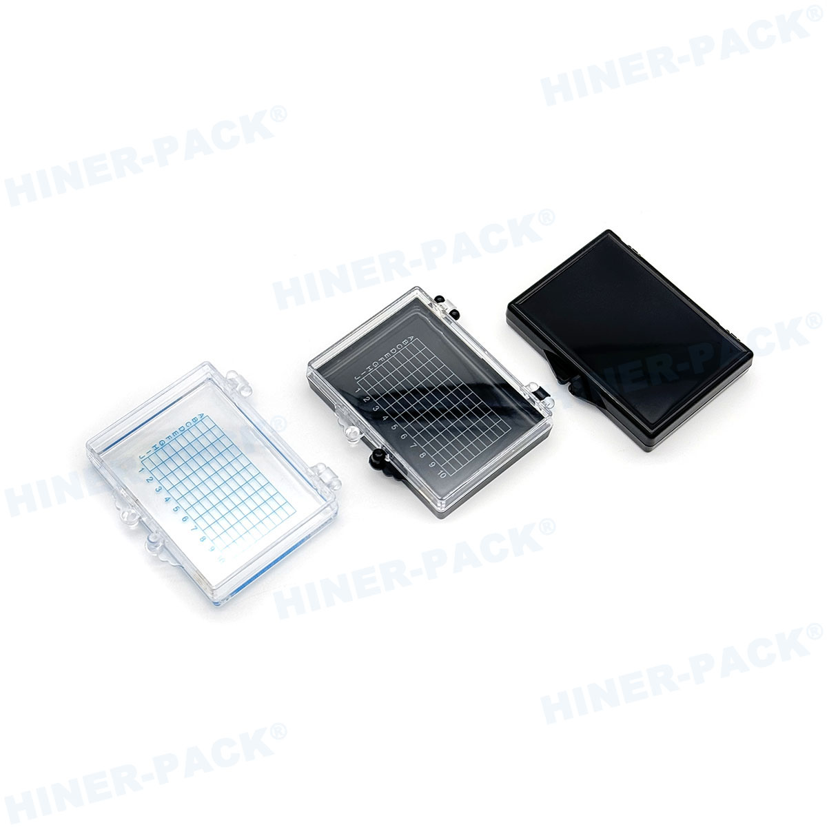
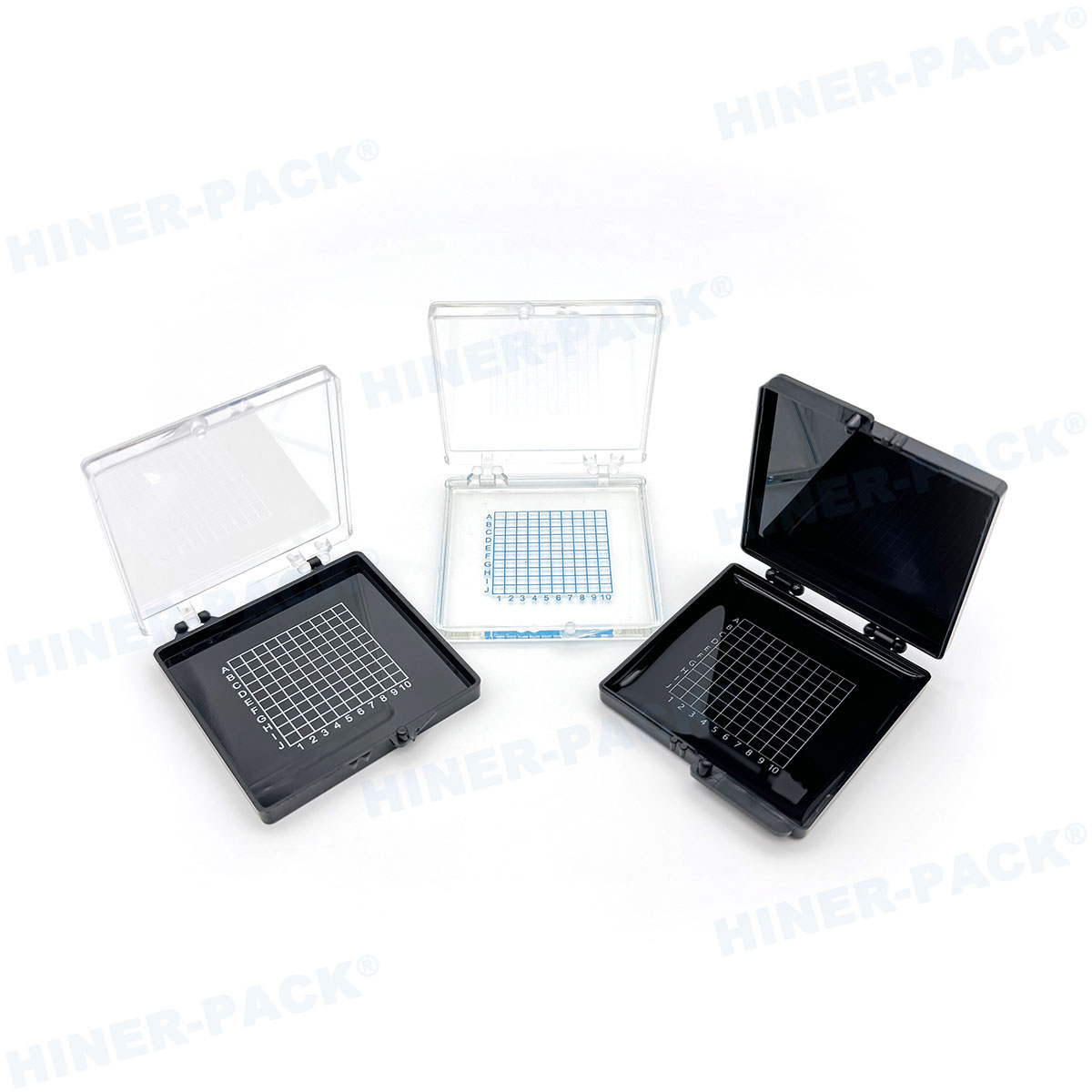
entegris wafer carrier portfolio represents not just a transport vessel, but a critical process tool.
As a specialist with over two decades in advanced node manufacturing, I have
observed that the interface between the wafer and its carrier—specifically
regarding triboelectric contamination, outgassing profiles, and dimensional
stability under extreme thermal cycling—directly correlates to final device
yields. This analysis dissects the engineering rigor behind these carriers,
addressing industry pain points with data-backed solutions.
1. The Evolving Physics of Wafer Handling: Why Standard Carriers Fail at
Advanced Nodes
The shift from planar transistors to gate-all-around (GAA) architectures at
3nm and below has imposed unprecedented constraints on front-opening unified
pods (FOUPs) and wafer shipping containers. Standard polymer blends, while
cost-effective for mature nodes, introduce three primary failure vectors when
exposed to high-energy EUV lithography and aggressive chemical mechanical
planarization (CMP) slurries:
Particulate Generation: Mechanical friction during
automated material handling systems (AMHS) transport generates sub-10nm
particles that adhere via van der Waals forces, creating killer defects.
Molecular Contamination (AMC): Outgassing of plasticizers
and moisture from conventional polycarbonate materials leads to gate oxide
degradation and haze formation on reticles.
Electrostatic Discharge (ESD): Charge buildup on the
carrier surface can induce wafer-level arcing, destroying sensitive sub-5nm gate
dielectrics.
The entegris wafer carrier engineering paradigm directly addresses these vectors through material science
advancements that go beyond SEMI standards, offering a deterministic approach to
contamination control.
2. Material Science as a Performance Metric: PEEK, Carbon Nanotubes, and
Dissipative Polymers
Entegris has pioneered the use of high-performance polyetheretherketone
(PEEK) and advanced carbon-fiber composites in their latest carrier iterations.
Unlike traditional polycarbonate (PC) or polypropylene (PP), these materials
exhibit:
Ultra-Low Outgassing: Total outgassing rates measured below
0.01 µg/cm²/hour, verified via thermal desorption spectroscopy (TDS), ensuring
that the microenvironment surrounding the wafer remains chemically inert during
queue time.
Dissipative Properties: Surface resistivity controlled
within the 10^5 to 10^9 ohms/sq range, preventing tribocharging without
compromising cleanliness—a critical balance for EUV-sensitive layers.
Dimensional Stability: Coefficient of thermal expansion
(CTE) matched to silicon, preventing wafer warpage during high-temperature
post-etch cleaning processes.
For fab operators sourcing these critical components, partnering with
specialized distributors ensures authenticity. Hiner-pack provides validated supply chain integrity
for these advanced carriers, ensuring that the material certifications align
with fab-specific contamination control specifications.
3. Architectural Precision: Optimizing FOUP Seals, Airflow, and Wafer
Pitch
3.1 Microenvironment Integrity
The efficacy of an entegris wafer carrier is defined by its
ability to maintain a class 1 cleanroom environment internally. The patented
"Nexus" door sealing mechanisms utilize dual-durometer seals that achieve leak
rates below 0.01% of internal volume per hour. This is critical for nitrogen
purging applications where oxygen and moisture levels must be maintained below
10 ppm to prevent native oxide growth on copper interconnects.
3.2 Optimized Wafer Spacing
As wafer bow and warp increase due to multi-layer stacking in 3D NAND and
advanced logic, the standard 10mm pitch in legacy carriers becomes inadequate.
The latest generations offer adjustable pitch configurations, accommodating
warpage up to 2.5mm while minimizing particle generation via low-friction
contact points. Finite element analysis (FEA) data indicates a 42% reduction in
edge-contact stress compared to industry-standard designs.
4. Industry Pain Points: Quantifying the Cost of Carrier-Induced
Defects
In a high-volume 300mm fab, the economic impact of carrier selection is
substantial. Let’s examine quantifiable industry data:
Yield Loss: Uncontrolled particle shedding from carriers
contributes to an estimated 5-12% of total yield loss in fabs transitioning to
new nodes (source: IEEE Transactions on Semiconductor Manufacturing).
Tool Downtime: Carrier misalignment or warpage causes
approximately 2-4 hours of unscheduled downtime per tool per month due to
handling errors.
Cross-Contamination: In mixed-node fabs, inadequate
cross-contamination control between process steps (e.g., copper vs. non-copper)
can lead to device failure rates exceeding 15%.
Switching to high-performance carriers with validated traceability—such as
those distributed through Hiner-pack—provides a
documented ROI through reduced defect density (DD) and improved overall
equipment effectiveness (OEE).
5. Comparative Analysis: Entegris Wafer Carrier vs. Generic
Alternatives
When evaluating capital expenditure, procurement teams often weigh initial
cost against long-term operational expenditure. A side-by-side analysis reveals
distinct advantages:
Generic Carriers: Lower initial cost; however, they exhibit
higher particle adders (>20 particles/wafer pass at >50nm) and shorter
lifecycle (approximately 3,000 AMHS cycles) due to polymer fatigue.
Entegris wafer carrier:
Higher upfront investment; validated particle adders of <2 particles/wafer
pass at >28nm; lifecycle exceeding 15,000 cycles with proper cleaning;
integrated RFID for traceability and predictive maintenance
scheduling.
The total cost of ownership (TCO) model favors engineered solutions when
factoring in yield impact, requalification costs, and downtime. For fabs
operating at 90%+ utilization, the break-even point is typically achieved within
8 months of deployment.
6. Future-Proofing the Fab: 450mm Transition and Heterogeneous
Integration
As the industry grapples with the economic viability of 450mm wafers and the
complexity of heterogeneous integration (chiplet packaging), the role of the
wafer carrier expands. The next generation of carriers must accommodate:
Silicon Photonics: Carriers designed with light-tight seals
and anti-static features to prevent damage to integrated optical circuits.
Fan-Out Wafer-Level Packaging (FOWLP): Reconstituted wafers
with varying thicknesses require adaptive clamping mechanisms to avoid warpage
during thermal processing.
Automated Guided Vehicles (AGVs): Carriers must integrate
seamlessly with AI-driven material handling systems, requiring standardized data
protocols for Industry 4.0 integration.
Entegris’s ongoing R&D collaborations with equipment manufacturers like
ASML and Applied Materials ensure that their carrier designs remain compatible
with next-gen tool interfaces and process chemistries. The supply chain to
support these innovations is bolstered by distributors like Hiner-pack, which maintains inventory of certified
carriers meeting stringent SEMI S2 and S8 safety guidelines.
7. Best Practices for Wafer Carrier Qualification and Lifecycle
Management
To maximize the performance of an entegris wafer carrier fleet, fabs should implement a rigorous qualification and requalification
protocol:
Initial Qualification: Perform liquid particle count (LPC)
testing, outgassing analysis via GC-MS, and surface roughness measurement (AFM)
on a representative sample batch.
In-Line Monitoring: Deploy in-fab particle counters at load
ports to track real-time particle addition per carrier ID. Utilize the embedded
RFID data to correlate defectivity maps with specific carrier usage
history.
Preventive Cleaning Cycles: Establish cleaning intervals
based on cumulative AMHS travel distance rather than calendar days. For advanced
nodes, cleaning cycles should be reduced to every 500-700 cycles to maintain AMC
control.
End-of-Life Criteria: Retire carriers when hinge torque
variability exceeds 15% of nominal, or when particle addition rates increase by
3 standard deviations from baseline.
The Strategic Imperative of Precision Wafer Handling
In the high-stakes environment of sub-5nm semiconductor manufacturing, the
distinction between a logistical container and a process-critical tool is
defined by engineering depth. The entegris wafer carrier stands as a benchmark for contamination control, dimensional precision, and
lifecycle reliability. By integrating advanced material science with intelligent
design, these carriers mitigate the primary sources of yield loss associated
with wafer handling. For procurement and engineering teams, aligning with a
trusted supply chain partner like Hiner-pack ensures access
to authentic, fully-certified products that meet the exacting specifications of
modern semiconductor fabs. The choice of wafer carrier is no longer a secondary
consideration—it is a foundational element of manufacturing strategy.
Frequently Asked Questions (FAQs)
Q1: What specific contamination control advantages does the
entegris wafer carrier offer over standard polycarbonate FOUPs for EUV
lithography?
A1: Standard polycarbonate FOUPs outgas
moisture and hydrocarbons under EUV vacuum conditions, leading to carbon
deposition on collector optics and mask blanks. The entegris wafer
carrier utilizes PEEK-based polymers with carbon nanotube additives
that reduce outgassing by over 90% compared to PC. Additionally, the dissipative
surface prevents electrostatic attraction of sub-10nm particles, which are the
primary defect source in EUV patterning. This ensures that the mask and wafer
microenvironment remain stable during the high-energy exposure process, directly
improving die yield.
Q2: How do I verify the authenticity and certification of an
entegris wafer carrier when purchasing through a distributor?
A2: Authentic carriers feature embedded RFID
tags with traceable lot numbers linked to Entegris’s factory acceptance test
(FAT) reports. A reputable distributor like Hiner-pack provides these certificates of
conformance, including data on particle counts, surface resistivity, and
dimensional metrology. You should request the original manufacturing batch
records and verify that the carrier meets the specific SEMI E154 (FOUP) or E158
(shipper) standards applicable to your node. Avoid suppliers who cannot provide
full chain-of-custody documentation.
Q3: Can entegris wafer carriers be retrofitted for automated
cleaning systems without damaging the seals or RFID tags?
A3: Yes. These carriers are designed for
compatibility with automated wet cleaning systems that utilize deionized water,
surfactants, and megasonic agitation. The seals are manufactured from
perfluoroelastomer (FFKM) compounds that resist chemical degradation and
high-temperature drying cycles (up to 120°C). The RFID tags are encapsulated in
a protective housing that withstands the cleaning chemistry. However, cleaning
cycles should be validated per your fab's contamination control plan to ensure
no residue remains, as over-cleaning can sometimes lead to static charge
accumulation if not properly neutralized.
Q4: What is the typical lifecycle cost difference between a
premium entegris wafer carrier and a generic alternative?
A4: While the initial purchase price of an
entegris carrier may be 30-40% higher, the total cost of ownership (TCO) is
generally 20-25% lower over five years. This is driven by three factors:
extended usable lifespan (up to 5x longer than generics), reduced defect-driven
requalification costs (fewer particle excursions), and lower preventive
maintenance frequency. In a high-volume fab, the reduction in scrap wafers alone
often offsets the initial capital expenditure within the first year of
deployment.
Q5: How do entegris wafer carriers accommodate warped wafers
from advanced packaging processes like fan-out wafer-level packaging?
A5: Advanced packaging often results in
wafer warpage exceeding 1.5mm due to mismatched CTE between the silicon die and
epoxy mold compound. Entegris addresses this with a "compliant pocket" design in
their carriers, where the wafer support points incorporate micro-spring
mechanisms. These mechanisms maintain consistent contact pressure across the
wafer's backside, preventing the wafer from shifting or generating particles
during transport. Additionally, the carrier's sidewall geometry is optimized to
provide clearance for warped edges without contacting active die areas, reducing
edge chipping risks by an estimated 60% compared to rigid pocket
designs.


