
In advanced semiconductor assembly and test, the physical handling of bare die, MEMS sensors, and compound semiconductor chips demands packaging that prevents die shift, mechanical abrasion, and electrostatic damage. Unlike rigid JEDEC trays or waffle packs, a gel pak box utilizes a tacky, low-outgassing gel layer to immobilize fragile components without vacuum holes or edge clips. This article provides a deep engineering analysis of gel-based carriers, focusing on material science, vacuum release mechanisms, and contamination control, drawing on expertise from Hiner-pack in precision semiconductor logistics.

1. Operating Principle and Inner Architecture of a Gel Pak Box
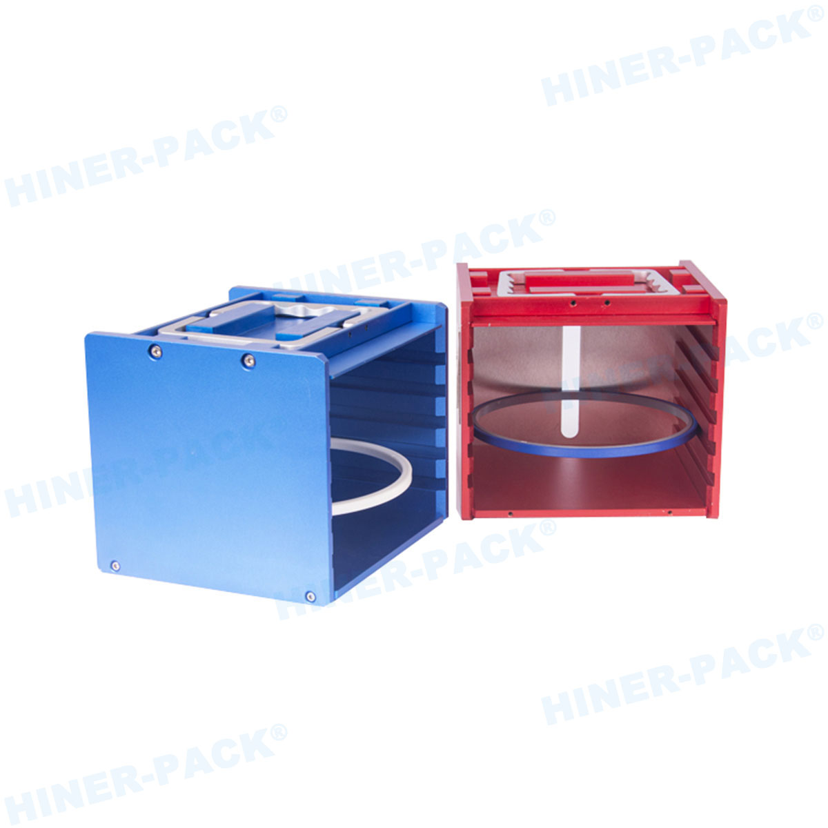
A gel pak box consists of three functional layers: a rigid outer carrier (typically anti-static polycarbonate or ABS), a conformal gel adhesive membrane, and a backing film that allows vacuum release. The gel layer, usually a silicone or polyurethane formulation with controlled tackiness (peel strength of 5–15 g/mm), gently holds the die by van der Waals forces. To remove a component without mechanical prying, operators apply a vacuum from underneath the box through a small port; the suction pulls the flexible gel membrane downward, breaking the adhesive contact and leaving the die free for pick-and-place equipment. This vacuum release technology eliminates tweezer damage and die edge chipping.
Key design parameters for a gel pak box include gel hardness (Shore A 20–40), surface resistivity (10⁹–10¹¹ Ω/sq for ESD dissipation), and cavity depth tolerance (±0.05 mm). Advanced models integrate conductive carbon-fiber fillers to prevent tribocharging during shipping, verified per ANSI/ESD STM11.11. The box lid often includes a desiccant pocket and a humidity indicator card to maintain dry environment (<5% RH) for moisture-sensitive devices.
2. Critical Application Scenarios for Gel-Based Die Carriers
Compared to waffle packs and JEDEC trays, the gel pak box excels in scenarios where mechanical restraint is impossible or risky. Typical use cases include:
Ultra-thin die ( < 100 µm ): Silicon die for 3D-IC or fan-out wafer-level packaging (FOWLP) easily crack in rigid pockets. The gel layer distributes holding force across the entire backside, preventing stress fractures.
MEMS micro-mirror arrays and accelerometers: Fragile moving structures (e.g., TI DLP chips) cannot tolerate edge contact. Gel immobilization avoids stiction damage.
Compound semiconductor die (GaN, SiC, InP): These materials are brittle and often have non-uniform backside metallization. Conformal gel adapts to surface topography without point loading.
Hybrid bonding test vehicles: Die with copper hybrid bonding pads require particle-free storage. Gel paks with low particle generation (< 200 particles >0.5 µm per box) meet Class 1 cleanroom standards.
For high-mix assembly lines, gel pak boxes are available in standard JEDEC footprint sizes (2×2 inch to 4×4 inch) and custom cavity matrices, accommodating die from 0.5 mm to 25 mm. Suppliers like Hiner-pack offer laser-cut gel inserts for specific die dimensions, reducing lateral movement during air freight vibration.
3. Industry Pain Points and Material Solutions
Despite their advantages, conventional gel paks present four persistent challenges that engineers must mitigate through proper material selection and process control:
Pain Point 1: Gel residue transfer to die backside
Low-quality silicone gels may leave microscopic residues after hundreds of vacuum release cycles, interfering with die attach adhesive or solder wetting. Solution: Use platinum-catalyzed silicone gels with low molecular weight cyclics (<0.1% extractables) or perfluoropolyether (PFPE) based gels. Verification via FTIR and ion chromatography ensures no silicone transfer after 50 releases. Gel pak box manufacturers now offer residue-free certification per SEMI F77.
Pain Point 2: Loss of tackiness after thermal cycling
Shipping across temperature extremes (-40°C to +85°C) can harden or soften gel, altering tack. Solution: Thermally stable urethane-acrylate gels with glass transition temperature (Tg) below -50°C maintain tack over 1,000 cycles. Request DMA (dynamic mechanical analysis) data from the supplier.
Pain Point 3: Outgassing contamination in hermetic packages
Volatile organic compounds (VOCs) from the gel can condense on optical surfaces or wire bonds. Solution: Specify low-outgassing gel paks tested per ASTM E595 (total mass loss <0.1%, collected volatile condensable materials <0.01%). For space-grade applications, use vacuum-baked gel boxes at 125°C for 24 hours before die loading.
Pain Point 4: Difficulty in automated die picking
Variation in vacuum release timing can cause incomplete separation. Solution: Choose gel pak boxes with integrated vacuum channels and a positive stop feature that limits membrane deflection. Automation-friendly designs include fiducial marks for vision systems and a uniform backside support plate.
4. Cleanroom Compatibility and ESD Performance Validation
For semiconductor fabs and OSATs, any consumable entering the cleanroom must pass strict particle, ionic, and ESD tests. A compliant gel pak box should provide documented evidence of:
Liquid particle count (LPC): After ultrasonic cleaning in DI water, the rinse water must show <50 particles ≥0.2 µm per cm² of gel surface.
Ionic contamination: Chloride, fluoride, sodium, and potassium ions each below 0.2 ppb per SEMI F59.
Surface resistivity: 10⁹ to 10¹¹ Ω/sq at 23°C, 12% RH (conductive polycarbonate case) and 10¹¹ to 10¹² Ω/sq for the gel itself.
Charge decay time: From ±1000 V to ±100 V in less than 2 seconds per ESD S11.11.
Hiner-pack manufactures gel pak boxes in an ISO 14644-1 Class 1000 cleanroom, with in-line ionized air rinsing and 100% visual inspection. Each batch includes a certificate of analysis (COA) summarizing particle count and ESD metrics.
5. Comparative Selection: Gel Pak Box vs. Waffle Pack vs. JEDEC Tray
Choosing the right carrier depends on die thickness, fragility, and automation level. The table below summarizes technical differentiators:
Die thickness support: Gel pak handles 25–800 µm; waffle pack minimum 200 µm; JEDEC tray only >300 µm.
Die shift during vibration: Gel pak: <0.1 mm; waffle pack: up to 1 mm; JEDEC tray: 0.5–2 mm (without insert).
Automation compatibility: Gel pak requires vacuum release system; waffle pack works with standard pick-and-place; JEDEC tray fully automated.
Cost per die (high volume): Gel pak: $0.20–0.80; waffle pack: $0.05–0.20; JEDEC tray: $0.01–0.05.
For prototype or low-volume production of sensitive dies (e.g., GaN power HEMTs or photonic integrated circuits), a gel pak box offers superior protection despite higher unit cost. Conversely, for standard QFN or BGA packages in high-volume, rigid trays are more economical.
6. Hiner-pack’s Engineered Gel Pak Solutions for Advanced Nodes
Recognizing the limitations of generic gel boxes, Hiner-pack has developed a series of application-specific gel paks addressing next-generation packaging challenges. Their product line includes:
Ultra-low outgassing series: With PFPE gel and fluoropolymer case, outgassing rate <5×10⁻⁵ mbar·L/s, suitable for vacuum-sealed MEMS gyroscopes.
High-temperature stable series: Silicone gel stable up to 150°C for die that require post-shipping bake.
Conductive gel series: Filled with nickel-coated graphite, surface resistivity 10⁵–10⁷ Ω/sq for ESD-sensitive RF die.
Each gel pak box from Hiner-pack is laser-marked with a unique QR code that links to production data (gel batch number, cleanroom validation date, and vacuum release test results). This traceability is mandatory for automotive (IATF 16949) and medical device manufacturing.
Frequently Asked Questions (FAQs)
Q1: Can a gel pak box be reused multiple times, and how to clean it?
A1: Reusability depends on gel integrity. High-quality silicone gel boxes can be reused 20–50 times if die are picked with vacuum release (never peel). Cleaning: Use only ionized air blow or isopropyl alcohol (IPA) wipe on rigid parts. Avoid contact with gel. Replace when tackiness reduces or residue appears. Single-use gel paks are also available for critical applications.
Q2: What vacuum level is required to release a die from the gel?
A2: Typically –40 to –70 kPa (relative to atmosphere) applied for 0.5–1 second. The exact value depends on gel thickness (0.5–2 mm) and die size. Too high vacuum may overstretch the membrane; too low fails to release. Hiner-pack provides a vacuum release calibration tool for each box type.
Q3: Are gel pak boxes compatible with 200mm and 300mm wafer handling?
A3: No – gel paks are designed for individual die or small chip arrays, not full wafers. For wafer transport, use wafer shippers or FOUPs. However, gel paks are often used after wafer dicing to ship singulated die from sawing to die bonding.
Q4: How to store gel pak boxes to maximize shelf life?
A4: Store in original sealed bag at 18–25°C, 30–50% RH, away from UV light and ozone. Do not stack more than 10 boxes high. Shelf life is typically 12 months from date of manufacture. After opening, use within 30 days to avoid contamination.
Q5: Can gel residue affect wire bonding or solderability?
A5: Yes, if the gel is not residue-free. Platinum-catalyzed silicone gels leave minimal residue, but for gold wire bonding or silver sintering, specify fluorinated gel or use a release liner between die and gel. Always perform a wire pull test on sample die from the first shipment.
Request a Technical Evaluation for Your Die Protection Needs
Selecting the correct gel pak box involves trade-offs among tack, outgassing, ESD protection, and automation compatibility. Hiner-pack offers free die sample testing – ship us 50 pieces of your fragile components, and our engineering team will recommend the optimal gel type, cavity pattern, and vacuum release parameters. We also provide custom gel die-cutting and cleanroom assembly services.
Contact our semiconductor logistics specialists today for a consultation or to request a sample kit. Send an inquiry →


