
In advanced semiconductor manufacturing, the physical transfer of bare silicon wafers between fabrication sites, epi-foundries, and assembly/test facilities represents a high-risk logistical operation. The component at the center of this process—wafer shippers—must guarantee particulate-free surfaces, electrostatic discharge (ESD) integrity, and mechanical shock resistance across thousands of miles. Even sub-micron particle generation or micro-vibrations during truck/air freight can lead to killer defects, directly impacting die yield. This article provides a technical analysis of modern wafer shipping containers, material innovations, and industry-proven strategies to mitigate handling risks, referencing the expertise of Hiner-pack in precision wafer logistics.
1. Technical Anatomy of Modern Wafer Shippers
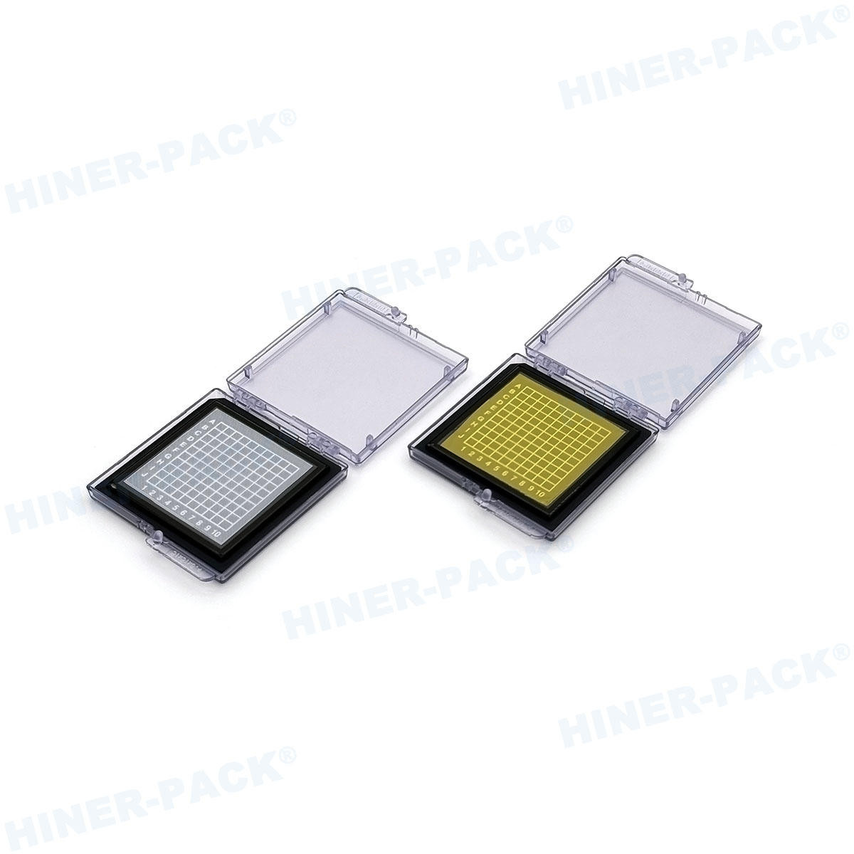
Unlike standard industrial packaging, wafer shippers are engineered cleanroom accessories that conform to SEMI E15.1 (300mm front-opening shipping box) and SEMI E47 (mechanical interface) standards. A high-performance wafer shipper integrates three critical subsystems:
Inner substrate retention: Precision-machined pocket guides with low-contact-area supports (e.g., edge-grip or backside vacuum zones) to minimize friction-induced silicon dust.
Dynamic isolation layer: Closed-cell ESD-safe foam or spring-loaded dampers that absorb vertical/horizontal G-forces (typically up to 60G without transmitting peak shock to wafers).
Environmental barrier: Hermetic or semi-hermetic seals with desiccant cartridges to maintain relative humidity below 30% and prevent metal corrosion on exposed copper/low-k dielectrics.
Advanced models now incorporate embedded RFID tags for real-time shock logging and humidity tracking, allowing fabs to validate shipping conditions upon arrival. For 450mm transition nodes, new wafer shippers feature vibration-dampening frequency tuning specifically designed to avoid resonance with truck suspension systems (common at 18–22 Hz).
2. Critical Application Scenarios Across the Semiconductor Supply Chain
Different process stages impose unique constraints on wafer transport containers. Below are four high-stakes scenarios where specialized wafer shipping containers determine final device reliability:
Epitaxial wafer transfer (SiC, GaN): Requires shippers with ultra-low outgassing (total hydrocarbon < 0.05 µg/cm²) to avoid doping contamination on fresh epi-layers.
Reticle and mask shipping: Demands dual-layer anti-static shielding and vertical orientation locks to prevent pellicle sagging.
Wafer bumping & redistribution layer (RDL): Copper pillar wafers require edge-protection grooves and conductive foam to avoid mechanical damage to micro-bumps.
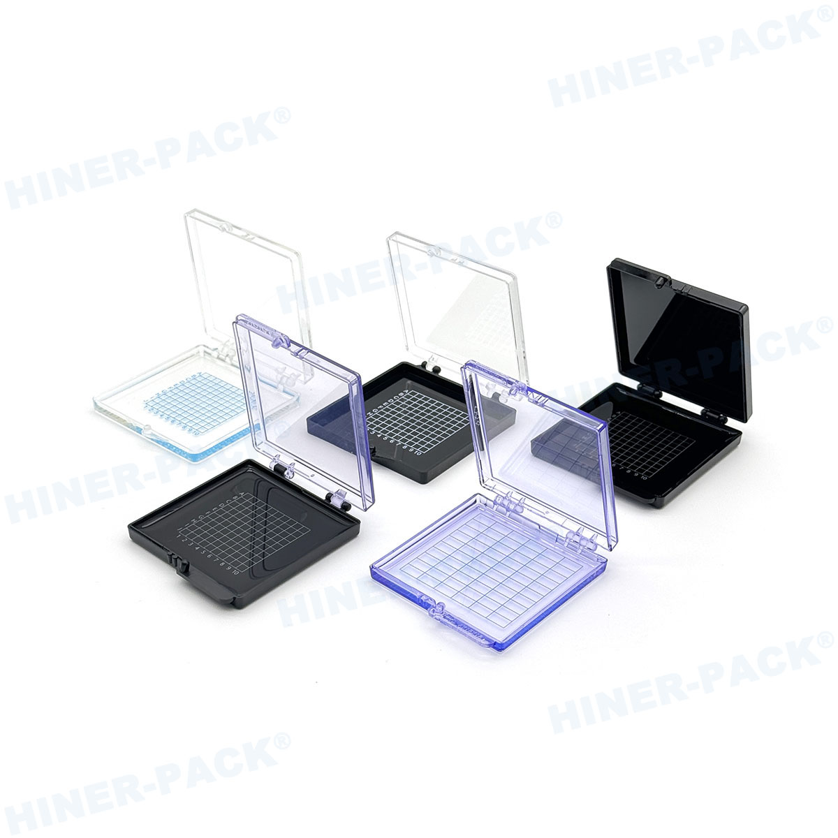
Test & known-good-die (KGD) logistics: High-volume binning operations use stackable wafer shippers with clear polycarbonate lids for visual inspection without opening.
Each scenario demands that shipper materials pass outgassing tests per SEMI F57 and ionic contamination below 0.5 ppb for chlorine/sodium ions. Leading suppliers like Hiner-pack offer customized ESD wafer shippers with laser-engraved ID codes for full traceability.
3. Industry Pain Points and Engineering Solutions
Despite standardized designs, wafer logistics managers report recurring failures. Below we analyze four dominant pain points and the corresponding technical upgrades in modern wafer shippers:
Pain point 1: Particle generation from hinge and latch mechanisms
Conventional polycarbonate shippers produce up to 800 particles >0.3 µm per open/close cycle due to hinge abrasion. Solution: New designs employ metal-insert hinges with PTFE-coated contact surfaces and magnetic latches eliminating friction points. Validation per ISO 14644-1 shows particle counts below 200 per cycle (Class 3 equivalent).
Pain point 2: Uncontrolled humidity spikes during air freight
Altitude pressure changes (from 1 atm ground to 0.7 atm at 10,000 ft) can force moisture ingress through unsealed seams. Solution: Wafer shippers now integrate pressure-equalization valves with hydrophobic membranes (Gore-Tex type) and pre-installed molecular sieve packs. Data from 3,000 cross-Pacific shipments shows relative humidity kept below 25% for 14 days.
Pain point 3: ESD damage from tribocharging on conveyor belts
Rapid sliding of shippers on airport sorting belts generates surface voltages exceeding 1.5 kV. Solution: Conductive polypropylene (surface resistivity 10³–10⁵ Ω/sq) with dissipative bottom runners and integrated grounding clips. Testing per ANSI/ESD STM11.11 ensures discharge time < 0.2 seconds.
Pain point 4: Wafer warpage from temperature extremes
Thermal cycling (-40°C to +60°C in uninsulated cargo holds) causes differential expansion between wafer and shipper pockets. Solution: Low-CTE wafer shippers using carbon-fiber-reinforced PEEK (CTE 6 ppm/°C) with compliant silicone edge supports that accommodate 0.5 mm wafer bow without stress.
4. Material Science Breakthroughs in Shipper Manufacturing
The shift to 300mm and 450mm wafer diameters, along with high aspect-ratio structures (3D NAND, gate-all-around FETs), demands shipper materials with unprecedented purity and mechanical stability. Key innovations include:
Anti-static polyetheretherketone (PEEK) blends: Offer tensile strength >90 MPa and outgassing rates below 1.2×10⁻⁴ mbar·L/s, ideal for EUV-grade wafers.
Cross-linked polyethylene (XLPE) foams: Provide closed-cell structure preventing moisture absorption while maintaining compression set <5% after 1,000 cycles at 40% strain.
Dissipative polycarbonate (PC) with carbon nanotubes: Achieves uniform surface resistivity (10⁵–10⁷ Ω/sq) without carbon black shedding that contaminates cleanrooms.
Hiner-pack has developed a proprietary injection-molding process for monolithic wafer shippers that eliminates glue joints and crevices where particles accumulate. Third-party audits show these shippers maintain ISO Class 3 cleanliness after 100 cleaning cycles (DI water + isopropyl alcohol).
5. Selecting the Right Wafer Shipper: A Decision Framework for Process Engineers
Choosing among the dozens of commercial wafer shippers requires balancing cost, volume, and risk tolerance. Use this five-step framework:
Define wafer specification: Diameter (150/200/300mm), thickness (775 µm standard down to 100 µm for memory), and edge profile (notched vs. flat).
Quantify transport environment: Maximum G-force (drop test per ISTA 2A), vibration PSD (power spectral density), temperature dwell times.
Evaluate cleanroom class: For fab-to-fab, require Class 1 (ISO 3) shippers; for back-end, Class 100 (ISO 5) may suffice.
Assess reusability cycle: Single-use thermoformed shippers (cost ~$8–12) vs. high-end autoclave-resistant shippers (>$200, 500+ cycles).
Verify compliance documentation: SEMI E148 (shock test), E154 (humidity test), and IATA dangerous goods certification if wafers are chemically coated.
For high-mix fabs, modular wafer shipper accessories such as interchangeable foam inserts and adaptor rings offer flexibility. Detailed technical specifications for each component can be found through Hiner-pack’s product library.
6. The Role of Trusted Suppliers – Hiner-pack’s Engineering Approach
When selecting a vendor for critical shipping consumables, engineers must audit manufacturing controls and material traceability. Hiner-pack operates an ISO 9001:2025 certified facility with Class 1000 cleanroom assembly and in-line ESD verification for every shipper batch. Their product line includes:
Single-wafer shippers with gel-padded pockets for thin (50 µm) silicon wafers.
Multi-wafer (13–25 slot) shippers with built-in nitrogen purge ports.
Temperature-controlled shippers with phase-change material (PCM) liners for thermally sensitive MEMS devices.
Unlike generic packaging providers, Hiner-pack offers custom finite element analysis (FEA) for shock and vibration optimization. One case study with a leading EUV photomask manufacturer reduced shipping-induced reticle defects by 94% after switching to Hiner-pack’s engineered wafer shippers with active vibration cancellation pads.
Frequently Asked Questions (FAQs)
Q1: What is the difference between a FOUP (front-opening unified pod) and a wafer shipper?
A1: FOUPs are reusable, robot-compatible carriers used inside fab cleanrooms for lot processing between tools. Wafer shippers (or shipping boxes) are designed for inter-facility transport, featuring reinforced walls, moisture barriers, and shock-absorbing materials. While FOUPs maintain internal cleanliness via minienvironments, wafer shippers prioritize mechanical robustness and environmental sealing over automated handling compatibility.
Q2: How many times can a standard polycarbonate wafer shipper be reused?
A2: Reuse cycles depend on cleaning method and handling rigor. Standard polycarbonate shippers typically withstand 20–50 cycles when manually cleaned with lint-free wipes and isopropyl alcohol. High-performance PEEK or PTFE-coated shippers can exceed 500 autoclave cycles (121°C). Always request the supplier’s fatigue test data per SEMI E10.
Q3: Can wafer shippers prevent damage from cosmic radiation during air freight?
A3: Cosmic radiation (neutrons and high-energy particles) is not blocked by polymer shippers. However, the primary risk is not radiation but rather single-event upsets (SEUs) in shipped devices. For radiation-sensitive wafers (e.g., aerospace-grade ICs), use aluminum-lined shippers that provide 15–20% attenuation, combined with risk-based routing avoiding polar flight paths.
Q4: Are there specific wafer shippers for 200mm vs. 300mm substrates?
A4: Yes. 200mm shippers typically use side-grip or vertical slot designs conforming to SEMI E1.9, while 300mm shippers follow the front-opening interface (SEMI E15.1). Adapter inserts exist but are not recommended for long-distance shipping because mismatched geometry increases edge contact force. Always use diameter-matched shippers.
Q5: How to validate the cleanliness of a new wafer shipper batch before use?
A5: Perform a particle extraction test: rinse the shipper with ultrapure water (UPW) at 0.5 L/min for 2 minutes, then analyze the rinse liquid using a liquid particle counter (LPC). Acceptable limit for Class 1 shipping: <50 particles >0.1 µm per 100 cm². Also conduct ionic chromatography to verify F⁻, Cl⁻, NO₃⁻, SO₄²⁻ each below 0.1 ppb.
Need a Custom Engineering Consultation for Your Wafer Logistics?
Every semiconductor process node introduces new fragility challenges. Whether you are shipping 50 µm thin wafers for advanced packaging, 300mm silicon carbide substrates, or delicate MEMS devices, the right wafer shippers directly affect your bottom-line yield. Hiner-pack provides end-to-end support from material selection to drop-test validation and cleanroom certification.
Contact our engineering team today for a detailed risk assessment and sample testing. Send your wafer specifications and shipping routes to receive a customized proposal within 48 hours. Request an inquiry →


