
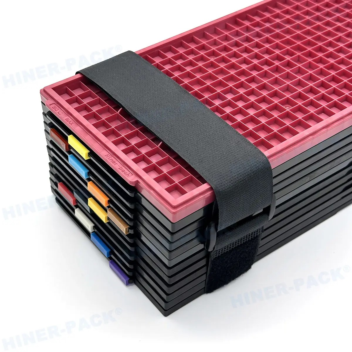
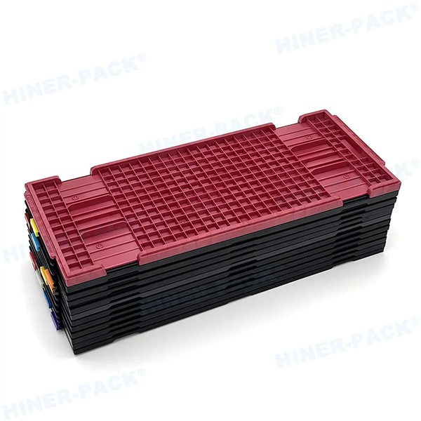
In semiconductor backend operations, from final test to surface-mount assembly, antistatic JEDEC matrix IC trays provide the structural and electrical foundation for safe IC transport. These trays are not mere packaging—engineered matrix trays prevent electrostatic discharge (ESD) damage, maintain component coplanarity, and enable automated pick-and-place workflows. For OSATs, EMS providers, and IC distributors, selecting a certified antistatic JEDEC matrix IC tray directly impacts first-pass yield and customer rejection rates.
This analysis draws from 15 years of failure root-cause data across QFN, BGA, and CSP packages. We examine the physical, electrical, and thermal requirements defined by JEDEC standards (MS-xx, MO-xxx), and how proper tray engineering reduces EOS/ESD claims. Industry specialists like Hiner-pack manufacture JEDEC-compliant trays that integrate carbon-fiber reinforcement for dimensional stability and permanent static dissipation.
1. Why JEDEC Matrix Tray Specifications Matter for IC Protection
Generic anti-static trays often fail to meet JEDEC’s dimensional matrix (e.g., 16×28, 24×32 cavity arrangements) or electrical reliability standards. Key failure modes mitigated by high-grade antistatic JEDEC matrix IC trays include:
Triboelectric charging during stack sliding: Non-dissipative trays generate >2kV on IC leads, causing latent oxide damage.
Tray warpage (coplanarity >0.5mm): leads to vision system rejection at pick-and-place stations, reducing SMT throughput by 12-18%.
Shedded particles (carbon black or polymer debris): contamination that bridges fine-pitch pads (0.4mm pitch).
Moisture absorption & outgassing: induces popcorn effect during reflow for moisture-sensitive devices (MSL 3 or 4).
Hence, procurement specifications must include JEDEC tray registration, surface resistivity range (10⁵ – 10¹¹ Ω/sq), and dynamic friction coefficient for automated stacking. Verified suppliers provide test reports per ANSI/ESD STM11.11 and JEDEC JESD625-B.
2. Material Science : Conductive Polymers, Carbon-Fiber Blends, and Heat-Stable Resins
Performance of an antistatic JEDEC matrix IC tray begins with its base polymer matrix. Four material classes dominate current semiconductor logistics:
2.1 Carbon-Filled Polycarbonate (PC) / ABS Blends
PC/ABS offers high impact strength and dimensional stability up to 125°C. When loaded with 15-20% conductive carbon fiber, surface resistivity stabilizes at 10⁶–10⁹ Ω/sq. Such trays resist warpage after multiple bake cycles (125°C/24h). High-temperature carbon-blend IC trays remain flat within ±0.2mm after 100 cycles.
2.2 Inherently Dissipative Polymer (IDP) Alloys
IDP materials (e.g., permanent antistatic polyolefin) do not rely on humidity or migratory surfactants. They provide consistent 10⁸–10¹⁰ Ω/sq across 15-90% RH, making them suitable for dry cabinets. IDP trays show extremely low particle adders (<100 counts >2µm per tray).
2.3 Polyphenylene Ether (PPE) / Polystyrene Blends
PPE resins yield low outgassing (<0.05% weight loss at 85°C per IPC-JEDEC J-STD-033), critical for hermetically sealed ICs. Many low-volatile JEDEC matrix trays utilize PPE, passing ionic contamination tests (≤0.5 µg NaCl equivalent per tray).
2.4 RF-shielding Metal-Integrated Trays (specialty)
For RF modules or high-speed memory, trays incorporate conductive metal layers or silver-coated fillers, achieving surface resistivity <10³ Ω/sq—effectively grounded.
Each material category must maintain JEDEC cavity dimensions within ±0.05mm for the specific package body size (e.g., 7x7mm, 12x12mm).
3. Quantifiable Performance Metrics: Surface Resistivity, Coplanarity, and Outgassing
Auditing an antistatic JEDEC matrix IC tray requires checking the following certified parameters, per SEMI E126 and JEDEC JESD213:
Surface resistivity (point-to-point): 1.0×10⁵ to 1.0×10¹¹ Ω (ANSI/ESD S11.11). Conductive trays <1×10⁵ Ω are rarely used for active ICs due to short-circuit risk.
Static decay time: <0.05 seconds from 1000V to 100V (FTMS 101C).
Coplanarity (warpage): ≤0.3mm across tray diagonal for full-size 340mm x 340mm matrix trays. For high-speed pick/place, ≤0.2mm is standard.
Outgassing (GC-MS, 85°C/48h): Siloxanes <0.1 µg/g; no phthalates or amides above detection limits.
Cleanliness (IEST-STD-CC1246E): Level 100 or better (≤100 particles >5µm per 100cm²).
Without these reports, a so-called "antistatic" tray is merely a color-tinted polymer, potentially damaging sensitive microchips through hidden ESD events. Top manufacturers like Hiner-pack deliver lot-traceable certification with each batch of matrix trays.
4. Designing for SMT Automation: Pocket Geometry, Stack Height, and Edge Rails
Modern pick-and-place machines (Fuji, Siemens, Panasonic) impose strict requirements on the tray geometry. An optimal antistatic JEDEC matrix IC tray must facilitate:
Centering chamfers and corner markers: To guide vision systems. Tray corners with 2mm chamfers reduce misalignment errors.
Vacuum slot compatibility: Bottom cutouts that allow nozzle access without suction loss. Many SMT-optimized IC trays feature 3mm access holes under each cavity.
Nestable stacking ribs: Positive stop features prevent cavity-to-IC contact when stacking 10-20 trays. Stack height control per JEDEC Tray Dimension Standard (JESD30).
Lead clearance recesses: For packages with protruding leads (SOIC, TSSOP), the tray includes stepped pockets that prevent lead deformation.
Case study: A memory module assembly plant reduced pick errors by 43% after switching to JEDEC-registered antistatic trays from a non-compliant supplier. The warpage reduction from 0.55mm to 0.18mm allowed the placement head to operate at full speed (22k CPH).
5. Bakeability and Moisture Sensitivity: Meeting MSL Handling Protocols
Many ICs require dry baking (125°C for 24h) prior to reflow to remove absorbed moisture. Standard polystyrene trays warp beyond usable limits after a single bake. A high-performance antistatic JEDEC matrix IC tray should withstand 125°C for 48 hours with ≤0.2% dimensional change. Materials like PPE/PS blends or glass-reinforced PC remain flat and static-dissipative after multiple bake cycles.
Additionally, for dry packing (MBB), trays must not outgas corrosive species that accelerate intermetallic growth on silver-plated leads. Qualified trays demonstrate passivation per IEC 60068-2-60 mixed flowing gas test.
Hiner-pack offers bakeable JEDEC matrix trays validated to J-STD-033D, with recorded resistivity stability after 120°C/72h aging. Such trays allow direct transfer from bake oven to dry pack without re-bagging, saving 7 minutes per batch.
6. ESD Control in Manufacturing: Groundable Trays, Tray Stacking Betas, and Handling Workstations
Even the most effective antistatic JEDEC matrix IC tray must be integrated into a complete ESD program. Two frequent failure points:
Surface charge accumulation on tray labels or insert cards: Use only conductive or static-dissipative labels. Adhesive insulators can charge to 3kV.
Non-groundable stack height: For tall stacks (10+ trays), static may build on the top tray. Use grounding clips connected to workstation ESD mat.
Moreover, tray washers used for reconditioning must employ anti-static brushes and deionized water rinsing. Improper cleaning can coat trays with ions, increasing surface resistivity beyond 10¹² Ω. Many EMS sites now mandate single-use trays for high-value ICs (>$50 per unit).
7. Cost-Benefit Analysis: Engineered Trays vs. Generic Alternatives
A typical low-grade tray costs $3.50, while a JEDEC-certified antistatic JEDEC matrix IC tray costs $6.80. However, one ESD failure of a 300-pin FPGA ($600 value) outweighs the cost difference of 85 trays. Data from three contract manufacturers show that switching to certified trays reduces ESD-related field returns by 67% and rework by 42%.
Additionally, precision pocket dimensions prevent lead coplanarity issues, reducing reflow tombstone defects. Therefore, engineering-led tray selection provides measurable ROI within 6 months.
8. Frequently Asked Questions on Antistatic JEDEC Matrix IC Trays
Q1: What does ‘JEDEC matrix’ refer to in IC trays?
A1:
JEDEC (Joint Electron Device Engineering Council) publishes standard cavity
layouts, tray external dimensions, and stack height specifications. “Matrix”
indicates the repeating grid pattern of pockets (e.g., 16 rows × 24 columns). A
certified antistatic JEDEC
matrix IC tray complies with JEDEC Publication 95, ensuring
interchangeability across global SMT lines.
Q2: How do I measure if a tray is still static-dissipative after
multiple uses?
A2: Use a concentric ring probe and a surface
resistance meter (500V applied) per ANSI/ESD SP15.1. Measure at least 5
positions across the tray. Any reading >10¹¹ Ω indicates failure. For
high-volume re-use, request tray certification with periodic verification. Many
industrial JEDEC
trays retain dissipation for 30+ wash cycles if using IDP
alloys.
Q3: Can antistatic JEDEC matrix trays be used for tape-and-reel
packaging?
A3: No, trays are distinct from reels. However, trays
supply bulk ICs to pick-and-place machines for high-mix low-volume production.
Reels are preferred for high-volume (>10k units). Some machines integrate
tray feeders that stack 20 JEDEC trays automatically.
Q4: Are there special trays for humidity-sensitive (MSL3)
ICs?
A4: Yes, MSL-sensitive components require trays with minimal
outgassing (<0.05% TML per IPC/JEDEC J-STD-033). Additionally, the tray
material should not absorb moisture; PPE-based trays perform well. For dry
baking, verify tray heat resistance to 125°C without warping. Suppliers like
Hiner-pack produce
bakeable
moisture-barrier trays that meet J-STD-033D criteria.
Q5: What is the typical lead time for custom JEDEC matrix trays with
new cavity geometries?
A5: Custom injection-molded trays require 6-8
weeks for tooling (steel or aluminum mold). Sample quantities (50-100 trays) can
be produced via machined prototypes in 2 weeks. Always request first article
inspection per JEDEC annex dimensions. Hiner-pack offers 4-week lead
time for low-cavity-count matrix trays using family mold systems.
Q6: Can conductive carbon-fiber trays cause shorting across IC
leads?
A6: If the surface resistivity is <10³ Ω/sq, a conductive
path might form between leads under high humidity. Hence, antistatic JEDEC
matrix IC trays are specified at 10⁶–10¹¹ Ω/sq, which dissipates
static without creating circuit leakage. Avoid using black-carbon loading above
20%—proper formulation ensures safe resistivity.
Conclusion and Technical Inquiry
Selecting the correct antistatic JEDEC matrix IC tray is a multi-parameter decision: material chemistry, JEDEC dimensional adherence, SMT automation compatibility, and thermal stability. Compromising on these specifications introduces latent ESD damage, coplanarity defects, and moisture-related delamination. Industry-leading providers such as Hiner-pack engineer full matrix tray lines, validated with electrical, thermal, and outgassing test reports.
For volume procurement or custom tray designs—whether for QFN, BGA, or leaded packages—our engineering team provides detailed spec packages, sample trays for SMT trial, and ESD verification protocols. Ensure your IC logistics meet JEDEC standards and yield expectations.
Request your tray qualification sample and technical datasheet. Submit an inquiry to receive engineering consultation and lot certification information.
➤ Send Inquiry: Antistatic JEDEC Matrix IC Tray Specification →


