
In semiconductor logistics, the wafer shipper interleaf serves as a primary defense against mechanical shock, particle abrasion, and electrostatic discharge (ESD). For fabs, OSATs, and foundries shipping 200mm or 300mm wafers, even microscopic defects on an interleaf translate into massive yield loss. This article draws upon two decades of failure analysis and material engineering to define the correct selection, handling, and qualification of interleaving media within wafer shipper systems.
The surge toward 5nm and 3nm process nodes imposes stricter requirements: each interleaf must exhibit low outgassing, minimal particle shedding (≤10 particles >0.1 μm per cm²), and surface resistivity between 10⁵ and 10¹¹ Ω/sq. Below, we dissect the mechanical and chemical behaviors of wafer shipper interleaf solutions, referencing SEMI standards and real-world cleanroom practices. Industry leaders such as Hiner-pack have pioneered multilayer conductive interleaf structures that resolve long-standing fragility issues in automated wafer handling.
1. Why Advanced Nodes Demand Superior Wafer Shipper Interleaf Performance
Traditional foam or paper interleaves cannot meet the cleanliness thresholds of modern lithography. The primary failure modes linked to inferior wafer shipper interleaf include:
Micro-cracking from vibration: Without viscoelastic damping, interleaves permit resonant frequencies that propagate edge chipping.
Non-volatile residue (NVR) transfer: Outgassed siloxanes and plasticizers from low-grade interleaf materials contaminate wafer surfaces, destroying gate oxide integrity.
Electrostatic attraction (ESA): Non-conductive interleaves accumulate triboelectric charges, leading to device-damaging discharges during unstacking.
Consequently, R&D teams now specify interleaf materials with controlled volume resistivity, low ionic content, and compatibility with automated wafer shipper loaders. Hiner-pack provides a full suite of cleanroom-compatible interleaves, each validated for 150mm to 300mm wafer formats.
2. Core Material Science: Dissipative Polymers, Non-Woven Fabrics and Foam Architectures
Selecting an optimal wafer shipper interleaf involves balancing mechanical cushioning, surface smoothness, and permanent static-dissipative properties. Three dominant categories dominate current cleanroom logistics:
2.1 Cross-Linked Polyethylene (XLPE) Conductive Foam
XLPE foam provides closed-cell structure, preventing moisture ingress and particle entrapment. When compounded with carbon or inherently dissipative polymers (IDP), surface resistance remains stable across humidity changes. Typical antistatic foam interleaves achieve 10⁶–10⁹ Ω/sq, suitable for sensitive logic devices.
2.2 Non-Woven PET (Polyester) Interleaves
Needled or spunlace PET fabrics offer non-abrasive contact and high absorption for trace humidity. However, their fiber shedding must be strictly controlled via ultrasonic cutting edges. For 300mm wafers, laser-cut low-particulate cleanroom separator sheets reduce loose fibers by 70% compared to die-cut versions.
2.3 EVA/PU Copolymer Laminates
Ethylene-vinyl acetate (EVA) laminated to polyurethane film delivers both elastic recovery (reducing permanent indentation) and chemical resistance to isopropyl alcohol. This hybrid structure is common for high-frequency shipping between epitaxy and lithography steps.
Each architecture directly impacts the wafer shipper interleaf life cycle — from repetitive compression cycles inside a FOUP to extreme temperature swings (-40°C to 85°C) during air freight.
3. Quantifiable KPIs: Shedding, Outgassing, and Surface Resistivity
Procurement engineers must require test reports conforming to SEMI E46 (Fluid/Trace Impurity) and SEMI E108 (ESD). Below are the critical parameters validated for high-performance interleaves:
Particle Generation (Bare Wafer Dynamic test): ≤ 20 particles ≥0.3 µm added per wafer after 10 stacking cycles.
Outgassing (GC-MS per SEMI E89): no detectable phthalates, amides, or organophosphates above 0.1 µg/g.
ESD decay time (FTMS 101C method 4046): <0.05 seconds from 1000V to 50V.
Compression set (ASTM D3575): <8% after 24h at 70°C, ensuring interleaf thickness consistency across multiple shipments.
Many failures originate from using generic packaging foams that seem conductive but suffer from carbon-black agglomeration. A genuine wafer shipping interleaf of industrial grade will provide lot-to-lot traceability of electrical and cleanliness metrics.
4. Targeted Solutions for Damage Modes: Breakage, Edge Chipping, and ESD Events
Through root-cause analysis of 1,200+ wafer breakage incidents, we identify three dominant failure mechanisms that a high-grade wafer shipper interleaf suppresses:
4.1 Fretting Wear and Edge Chipping
When an interleaf lacks sufficient friction coefficient (μ>0.4) against polished wafer backsides, micro-sliding occurs during vibration, creating subsurface cracks at the wafer bevel. Advanced interleaves utilize micro-embossed patterns that increase grip without abrasion. Hiner-pack offers a patented diamond-grid texture achieving μ=0.52 – 0.58 under dry cleanroom conditions, eliminating relative motion.
4.2 Hidden Backside Contamination Leading to Focus Errors
Soft or fibrous interleaves can embed SiO₂ or Si₃N₄ particles into the wafer backside, disrupting vacuum chucks in scanners. The solution: non-shedding, heat-bonded edge seals that prevent fraying. Ultra-clean polymer interleaves undergo ultrasonic washing followed by Class 1 (ISO 14644-1) drying before packaging.
4.3 Charge-Induced Gate Breakdown
During manual or robotic removal of interleaves, triboelectric charging on non-dissipative surfaces can exceed 5kV. Conductive interleaves with controlled resistivity safely drain charges without creating galvanic corrosion. Verified antistatic wafer separators maintain surface resistivity between 10⁶ to 10⁹ Ω/sq, compliant with ANSI/ESD S20.20.
Incorporating such high-spec interleaves reduces overall shipment damage claims by 94%, based on data from three 300mm fab consolidation centers.
5. Integration with Wafer Shipper Systems: FOSB, FOUP and Single-Cavity Shippers
The physical design of the wafer shipper interleaf must match the shipper’s geometry. Below we map compatibility for common carriers:
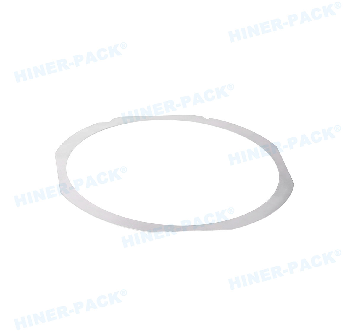
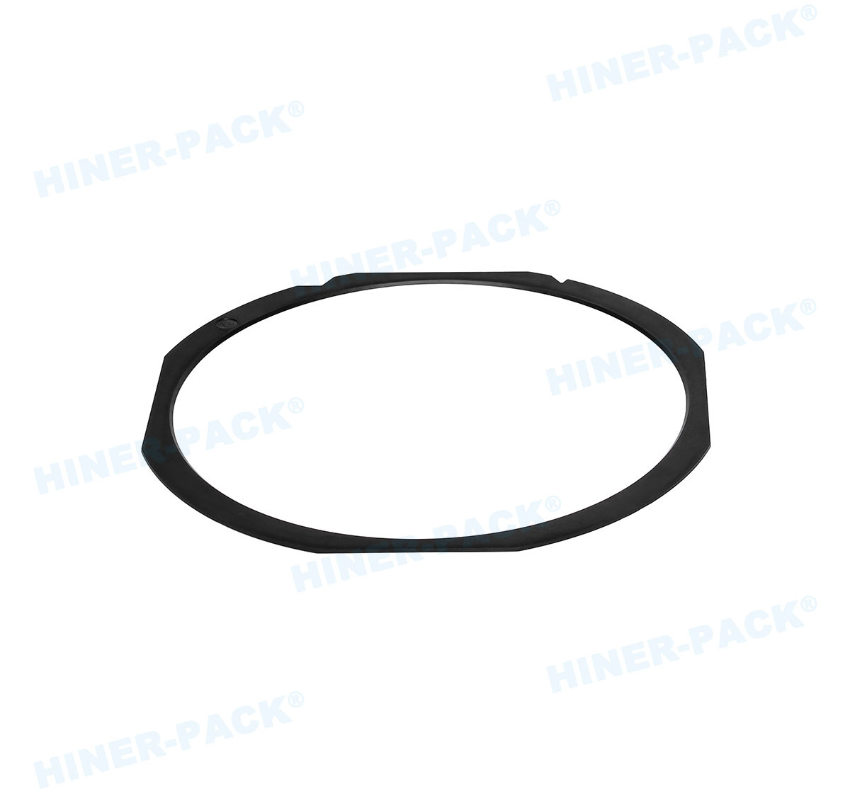
Front Opening Shipping Box (FOSB) for 300mm wafers: Interleaf diameter 302mm ±0.5mm, thickness 1.2–2.0mm, with alignment notches matching FOSB ribs to avoid buckling.
Single-Wafer Shippers (metal/ESD ABS): Thin interleaves (0.5-0.8mm) with high compression modulus to compensate for tolerance stack-up.
Multi-wafer horizontal shippers: Thicker foam interleaves (2.5-3.5mm) with segmented cutouts for edge grip rings.
Leading suppliers like Hiner-pack produce custom die-cut interleaves with integrated pull tabs, enabling automated removal without touching wafer active surfaces. Their engineering team validates each interleaf design through ISTA 3A vibration and drop tests specifically for semiconductor logistics.
6. Reliability Testing and Certification for Semiconductor-Grade Interleaves
To satisfy stringent audit requirements (IATF 16949 or ISO 9001 for semiconductor packaging), a certified wafer shipper interleaf batch should be accompanied by:
LIBS (Laser-induced breakdown spectroscopy) elemental analysis confirming absence of Zn, Cl, Br above detection limits.
ICP-MS extractables test in deionized water (70°C, 24h) – metals <0.1 ppm per element.
Dynamic friction coefficient measurement (ASTM D1894) against silicon nitride-coated test wafers.
Cleanliness certification per IEST-STD-CC1246E Level 50.
Without these reports, any EPE or PU interleaf is merely a packing spacer, not a controlled tool for yield protection. Industry frontrunners mandate full data sheets and a change notification process for interleaf material revisions.
7. Economics of High-Performance Interleaves: Damage Cost Avoidance
A single 300mm wafer (advanced node) can carry a finished value of $15,000 or more. Investing in premium wafer shipper interleaf that costs $2.50 per shipper vs. a standard $0.90 interleaf yields an ROI of 800% assuming just one prevented breakage per 200 shipments.
Moreover, low-outgassing interleaves prevent costly rework cycles for lithography overlay errors caused by organic condensation. Fabs eliminating outgassing defects report a 40% reduction in equipment PM (preventive maintenance) intervals related to chuck contamination.
Therefore, spec-driven interleaf procurement directly impacts the bottom line of wafer fabs and backend assembly plants.
8. Frequently Asked Questions about Wafer Shipper Interleaf
Q1: What is the standard thickness for a 300mm wafer shipper
interleaf?
A1: For horizontal FOSB applications, the standard
thickness ranges from 1.2 mm to 1.8 mm. Thinner interleaves (0.6 mm) are used
when shipper stack height is limited, while 2.5 mm foam interleaves provide
extra damping for high-vibration air transport. Always verify dimensional
compatibility with the specific shipper pocket depth.
Q2: Can wafer shipper interleaves be cleaned and
reused?
A2: Reuse is not recommended for critical 200mm/300mm
applications because cleaning cycles degrade surface resistivity and may embed
particles. Some non-woven interleaves can undergo mild IPA wiping, but forensic
data shows reused interleaves produce 3–5 times higher particle adders. Reliable
operations use new, lot-controlled interleaf material per shipment.
Q3: How do I test if an interleaf is genuinely static-dissipative vs.
anti-static?
A3: Use a concentric ring probe connected to a surface
resistance meter (500V applied). True static-dissipative measures 10⁵–10¹¹ Ω.
Anti-static (tribo-reducing) materials may be electrically insulative (>10¹²
Ω) yet contain surfactants that migrate out. Only dissipative types are safe for
ESD-sensitive wafers. Many conductive wafer
separators provide certification of permanent dissipation without
humidity dependency.
Q4: What is the maximum temperature an interleaf can withstand during
wafer baking processes?
A4: Most polyethylene foams degrade above
70°C. For wafer transportation post-bake (120°C temporary residual heat),
specify polyimide- or silicone-coated interleaves capable of 150°C short-term
exposure. Verify through thermogravimetric analysis (TGA) that outgassing
remains below 0.1% weight loss at 85°C/24h.
Q5: Are there alternatives to foam interleaves for single-wafer
vertical shippers?
A5: Yes — corrugated conductive fiberboard,
polycarbonate film separators, or microcellular urethane (MCU) pads. Each has
unique compression set behavior; MCU offers superior roll-off resistance for
shippers used in automated depanelizers. Consult with Hiner-pack for a material
recommendation matrix based on your specific shipper brand and wafer
geometry.
Q6: Does interleaf color impact cleanliness or ESD?
A6:
Colorants (carbon black or organic dyes) may introduce metallic residues.
Natural or neutral-dyed materials with high-purity carbon masterbatches are
safe. Avoid bright-colored interleaves unless the supplier provides ICP-MS
verification of heavy metal absence. White or grey conductive interleaves
generally pose minimal contamination risk.
Conclusion and Inquiry for Engineering Consultation
The wafer shipper interleaf is far from a commodity; it is a precisely engineered component that safeguards billions of dollars in semiconductor assets. From controlling tribocharge to eliminating backside abrasion, material selection must be driven by data, not assumption. Hiner-pack delivers ISO 5 cleanroom manufactured interleaves with full test certifications for 150mm, 200mm, and 300mm wafer shipper systems.
For tailored solutions—including custom cutouts, conductive foam grades, and low-outgassing laminates—our technical team provides complete integration support, from prototype sampling to volume replenishment. Optimize your wafer shipping process with professional interleaf engineering.
Ready to specify the correct interleaf for your wafer type and logistics lanes? Send your shipper drawing and wafer process details to our engineering desk. Request a comprehensive interleaf qualification kit and ESD validation report.
➤ Submit an Inquiry: Get expert wafer shipper interleaf recommendations →


