In the highly precise and contamination-sensitive world of semiconductor manufacturing, the humble carrier box for wafer fabrication (fab) plays an outsize role. These containers are far more than simple plastic boxes; they are the first and last line of defense for some of the most expensive and delicate components on earth. As wafer sizes have standardized on 300mm, the ecosystem of carriers designed to protect them has evolved into a sophisticated field of its own. This article delves into the pivotal carriers—the Front Opening Unified Pod (FOUP) and the Front Opening Shipping Box (FOSB)—that are foundational to modern fab operations. We will explore the SEMI standard carrier specifications that ensure global interoperability and examine the common challenges that can arise in their use, impacting yield, contamination, and ultimately, the bottom line.
The Backbone of Modern Fabs: Understanding the 300mm Wafer Carrier
The transition from 200mm to 300mm wafers was a monumental shift in the semiconductor industry, demanding a complete redesign of handling and storage solutions. The 300mm wafer carrier became the new standard, designed to handle the larger, thinner, and more valuable silicon wafers without damage. Unlike their smaller predecessors, these carriers are typically handled automatically by robotic systems to minimize human interaction and the associated risk of contamination.
A carrier box for wafer fabrication (fab) for 300mm wafers is engineered to be hermetically sealed, protecting its contents from environmental hazards like airborne molecular contaminants (AMCs), humidity, and particles. The internal environment is often controlled, sometimes filled with inert gases like nitrogen to prevent oxidation. The mechanical design is equally critical, ensuring precise alignment for robots to insert and retrieve wafers without contact, a process repeated thousands of times daily.
Front Opening Unified Pod (FOUP): The Fab Workhorse
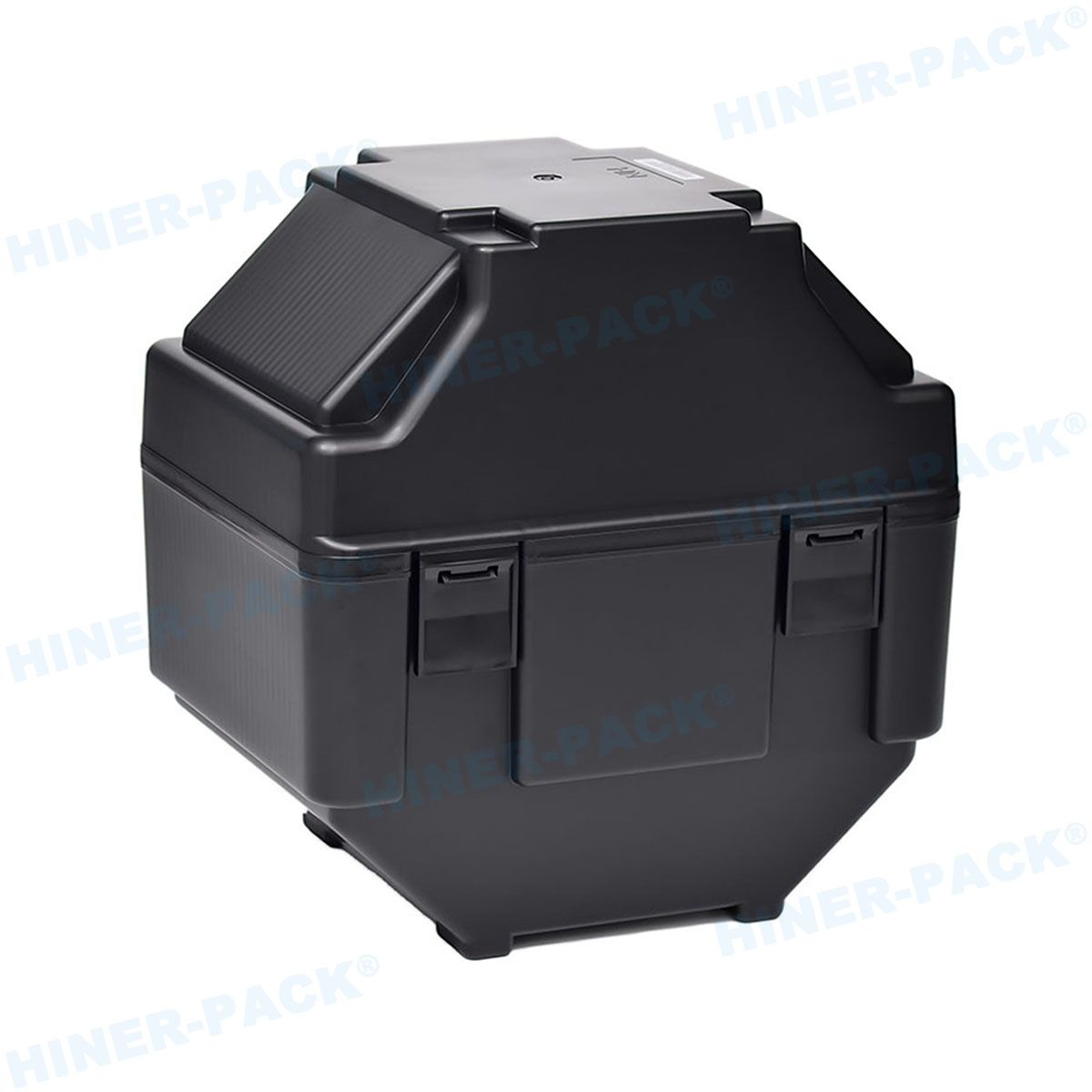
The Front Opening Unified Pod (FOUP) is the undisputed king of the cleanroom. It is the primary carrier box for wafer fabrication (fab) used for storing and transporting wafers within the semiconductor fabrication facility itself.
Design and Function
As the name implies, the FOUP features a single, large door on its front side. This design allows automated equipment (tool platforms) to open the door and access all 25 wafers inside simultaneously with a single, precise robotic arm. The door integrates a sophisticated latching mechanism that ensures a perfect seal every time it is closed. The FOUP's shell is made from advanced, static-dissipative polymers like PPS (polyphenylene sulfide) or PC (polycarbonate) that are incredibly clean, durable, and resistant to outgassing.
The Role of the FOUP
The FOUP's job is to be a "mini-environment." It moves from one processing tool to another on an overhead transport system, carrying its precious cargo. Each time it arrives at a tool, the tool's door opens, the FOUP's door opens, and the wafers are processed. The FOUP ensures that the wafers are only exposed to the highly controlled mini-environment of the tool and the inside of the pod itself, never to the cleanroom air, which, while clean, is not clean enough for advanced nodes.
Front Opening Shipping Box (FOSB): The Inter-Fab Courier
While the FOUP is designed for the controlled confines of a single fab, wafers often need to travel between different manufacturing sites, for example, from a fab to a separate test and assembly facility. This is the domain of the Front Opening Shipping Box (FOSB).
Key Differences from the FOUP
At first glance, a FOSB looks very similar to a FOUP. However, it is built to be significantly more robust. Its mission is to withstand the rigors of international shipping—handling by humans, vibrations, shocks, and significant changes in temperature and pressure.
Robustness: FOSBs have thicker walls and more reinforced structural elements.
Sealing: They feature more robust sealing gaskets to maintain a hermetic seal under non-ideal conditions, often validated to withstand pressure differentials experienced during air transport.
Containment: A key function is to contain any hazardous materials if the wafers have been processed with chemicals; it must be safe for handlers outside the cleanroom.
The FOSB is essentially a heavy-duty, shipping-grade version of a FOUP. It protects the wafers during their journey and is then unloaded in a receiving cleanroom, where the wafers are transferred into standard FOUPs for processing.
The Glue of the Industry: Adherence to SEMI Standard Carrier Specifications
The seamless operation of a global semiconductor supply chain would be impossible without standardization. This is where the SEMI standard carrier comes in. SEMI (Semiconductor Equipment and Materials International) is the global industry association that sets standards for the industry.
SEMI standards (e.g., SEMI E1.9, E15.1, E47.1, E62) define every critical aspect of a 300mm wafer carrier:
Physical Dimensions: The exact outer dimensions, ensuring it fits on every tool's load port and every stocker shelf.
Kinematic Coupling: The precise notches and grooves on the bottom that allow robots to pick up and position the carrier with micron-level accuracy.
Door Design: The latching mechanism, flange dimensions, and interface are standardized so that any FOUP can open on any tool from any manufacturer.
Radio-Frequency Identification (RFID): The location, type, and protocol for the RFID tag are standardized, allowing for automated tracking of wafers through the fab.
This standardization is what allows a carrier from Company A to be used flawlessly on a tool from Company B in a fab owned by Company C. It is the universal language of wafer logistics.
Common Challenges and Problems with Wafer Carrier Boxes
Despite their advanced design and strict standards, issues with carrier boxes for wafer fabrication (fab) can and do occur, leading to costly downtime and yield loss.
1. Particulate Contamination Generation and Retention
This is the most persistent and critical problem. Over time, carriers can themselves become a source of contamination.
Wear and Tear: Repeated robotic handling can cause microscopic wear on the bottom kinematic couplings and the interior wafer slots, generating particles.
Outgassing: Lower-quality plastics or materials degraded by chemical exposure can outgas, depositing films on wafer surfaces.
Improper Cleaning: If not cleaned correctly and frequently using validated wet bench or automated systems, particles and residues accumulate inside the pod.
2. Mechanical Damage and Misalignment
Dropped Carriers: Even a minor drop can misalign the kinematic couplings or crack the shell, compromising the seal and robotic handling.
Slot Wall Damage: Mishandled wafers or incorrect robot teaching can scratch or crack the delicate wafer slots, leading to particle generation and potential wafer misplacement.
3. Electrostatic Discharge (ESD)
While carriers are made from static-dissipative materials, improper handling or environmental conditions can lead to a build-up of static charge. This charge can attract airborne particles to the wafer surface like a magnet or, in worst-case scenarios, cause an ESD event that damages sensitive circuits.
4. Door Seal and Latching Failures
The integrity of the door seal is paramount. A failure here renders the entire mini-environment concept useless.
Worn Gaskets: The door gasket can wear out, tear, or become contaminated, preventing a proper seal.
Faulty Latch Mechanism: A misaligned or broken latch will not secure the door, risking it opening unexpectedly or failing to seal.
5. Cross-Contamination
When a carrier is used for multiple process steps, residual chemicals from one process can remain inside the pod and interact with wafers in a subsequent, incompatible process. This necessitates strict carrier dedication or ultra-effective cleaning procedures for certain process tools.
6. RFID and Tracking Issues
A faulty, dirty, or dead RFID tag can cause a carrier to be misidentified or lost in the automated material handling system (AMHS), bringing production to a halt until it is located manually.
Mitigation and Best Practices
The industry combats these problems through rigorous protocols:
Preventive Maintenance: Regular, scheduled inspection and replacement of carriers based on usage cycles.
Advanced Cleaning: Automated cleaning systems use precise chemistries and DI water to thoroughly decontaminate carriers without damaging them.
Comprehensive Metrology: Using specialized tools to scan for particles inside empty carriers, measure outgassing, and verify the health of RFID tags.
Strict Handling Procedures: Training and automated systems minimize opportunities for human error and mechanical damage.
The ecosystem of carrier boxes for wafer fabrication (fab), centered on the 300mm wafer carrier, is a masterpiece of engineering and standardization. The Front Opening Unified Pod and Front Opening Shipping Box, governed by unwavering SEMI standard carrier specifications, form the invisible logistics network that makes modern semiconductor manufacturing possible. They are the silent guardians of the technological world, ensuring that the wafers that become the brains of our devices are protected from the factory to the far corners of the globe. Understanding their function, standards, and potential pitfalls is not just a niche concern—it is fundamental to understanding how the digital age is built, one wafer at a time. As fabs move to even larger wafers and more advanced processes, the evolution of these critical carriers will continue to be a key enabler of progress.


