Quad Flat No‑lead (QFN) packages have become a dominant choice for analog,
power management, and RF devices due to their excellent thermal performance,
small footprint, and low inductance. However, the absence of formed leads
exposes the side-wall terminations and the bottom thermal pad to mechanical
damage, electrostatic discharge (ESD), and contamination during shipping,
baking, and surface-mount assembly. The primary carrier for high‑volume QFN
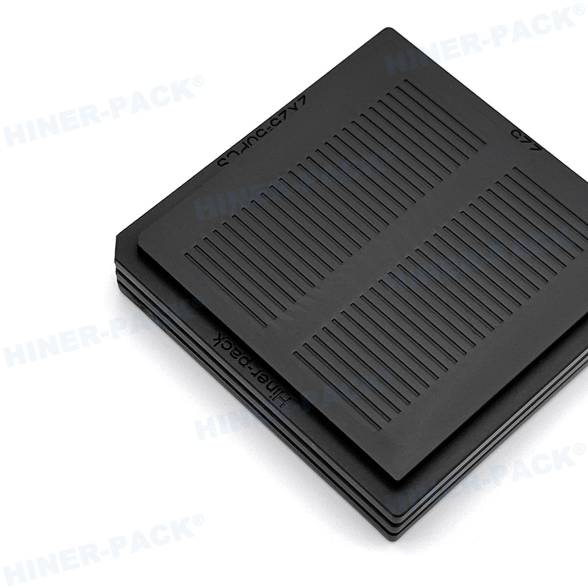
handling is the QFN jedec matrix IC
trays, a precision‑molded platform that follows JEDEC Publication
95 design guidelines while addressing the specific needs of leadless packages.
This article provides a detailed technical overview of JEDEC matrix tray
specifications, pocket geometry optimization, material selection trade-offs,
industry failure modes, and validated solutions from Hiner-pack, a specialist in
semiconductor handling products.
1. Why QFN Packages Demand Specialized JEDEC Matrix Trays
Unlike BGA or QFP packages that have protruding balls or gull‑wing leads, QFN
components have flush terminations on the bottom side and exposed copper pads on
the package edges. This construction introduces two handling
vulnerabilities:
Terminal damage: Solder‑plated side pads can be scraped or
deformed by rough pocket walls, leading to poor wetting during reflow.
Thermal pad contamination: Dust or fibers trapped in the
pocket can adhere to the exposed center pad, causing voiding or thermal
resistance increase.
Standard QFN jedec matrix IC
trays incorporate design features specifically for leadless
packages: chamfered pocket entrances, smooth side‑wall surfaces (Ra ≤ 0.8 µm),
and stepped pocket floors that support the package body without contacting the
terminations. These features are defined in JEDEC Tray Standard MO‑xx variants
but are often customized by experienced tray manufacturers to match exact QFN
body dimensions (e.g., 3×3 mm, 5×5 mm, 7×7 mm).
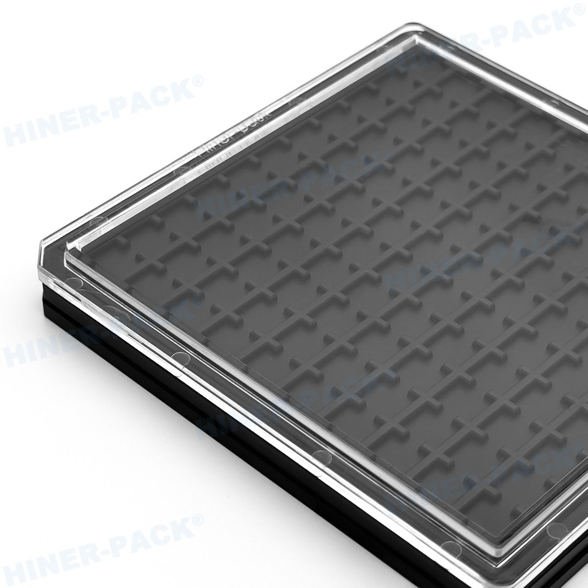
2. Key Technical Parameters for QFN Jedec Matrix Trays
Selecting QFN jedec matrix IC
trays requires evaluating five interrelated parameters that affect
yield in backend and SMT lines.
2.1 Pocket Depth and Terminal Clearance
For a QFN with body height of 0.85 mm (typical for 1 mm max height), the
pocket depth should be approximately 0.9 mm to 1.0 mm, leaving a 0.05–0.15 mm
gap above the package after sealing. This prevents vertical movement while
allowing vacuum nozzle pick up. The pocket side walls must be drafted (1° to 3°)
to avoid trapping the package edges. Most importantly, the pocket floor should
only contact the molded body region, not the side terminations. A well‑designed
tray leaves a 0.1 mm air gap around the four pads.
2.2 Warpage Control During Pre‑reflow Baking
QFN devices are moisture sensitive (typically MSL 2 or 3) and require baking
at 125°C for 24 hours before use. Tray warpage during this cycle can cause
nested trays to separate unevenly, ejecting components. JEDEC limits warpage to
≤0.3 mm per 300 mm length after thermal conditioning. For QFN trays, materials
with glass transition temperature (Tg) above 150°C are recommended: glass‑filled
PEI (Tg ~210°C) or reinforced PPS (Tg ~200°C). Hiner-pack offers QFN trays
molded from high‑flow PPS that maintain warpage below 0.12 mm after 125°C/48
hours.
2.3 ESD Control for Leadless Packages
QFN terminations are directly connected to internal bonding wires and die
pads. A static discharge as low as 500V can damage the ESD‑sensitive CMOS
structures in many QFNs. Tray surface resistivity must be within the
static‑dissipative range (10⁵ to 10⁹ Ω/sq) per ANSI/ESD S20.20. However, QFN
trays are often washed repeatedly; migratory antistatic agents can leach out.
Inherently dissipative polymers (IDPs) or carbon‑fiber filled materials provide
permanent ESD protection. Many ESD‑safe JEDEC matrix trays for
QFN packages use carbon loading that is evenly distributed through
injection molding.
2.4 Contamination Control (Particle and Ionic)
Because QFN terminations are not washed after tray assembly, any loose
particles (fibers, dust, mold release residue) that transfer to the pads can
cause solder non‑wetting. High‑quality trays are molded in ISO Class 7 or better
cleanrooms, using low‑outgassing materials that meet RoHS and REACH. After
molding, trays are ultrasonically cleaned in deionized water and tested for
ionic cleanliness (per IPC‑TM‑650).
3. Application Scenarios: From OSAT to SMT Line
QFN jedec matrix IC
trays are deployed in four main stages of the semiconductor supply
chain. Each stage imposes distinct requirements.
Outsourced assembly and test (OSAT) backend: After
singulation and marking, QFNs are placed into trays for electrical test and
vision inspection. Trays must have high flatness for automated handling by test
handlers (e.g., Advantest, Teradyne). Pocket position accuracy within ±0.05 mm
is required.
Dry‑pack and moisture barrier bag (MBB) storage: Trays are
stacked, placed in a vacuum bag with desiccant packs. Tray stack height must be
controlled to avoid crushing the bottom pockets. JEDEC defines stack height
limits based on tray rib design.
Pre‑baking and kitting: Many SMT lines dry‑bake QFNs at
125°C for 12–24 hours. Trays must survive without discoloration or release of
volatiles that could condense on solder pads. High‑temperature polyetherimide
(PEI) trays are preferred for repeated baking.
Direct tray feeding into pick‑and‑place machines: Modern
SMT lines use tray feeders (from Panasonic, Fuji, Mycronic) that index trays
under a vision system. Trays need high contrast (black or dark gray) and
anti‑glare surfaces. Also, chamfered corners and fiducial marks help optical
recognition.
Each application may require a different material grade. For example, OSAT
test handlers need maximum dimensional stability, while dry‑pack storage
prioritizes low moisture absorption and mechanical impact strength.
4. Industry Pain Points and Engineering Solutions
Despite JEDEC compliance, many assembly engineers report recurring problems
with QFN trays. Below are four high‑frequency pain points and countermeasures
derived from field data.
4.1 QFN Rotation and Snagging in Pockets
Pain point: QFN packages rotate within the pocket by up to
5° during shipping, causing pick‑up errors or wrong orientation. Rotation occurs
when pocket length and width are 0.2 mm larger than the package
body.
Solution: Reduce clearance to 0.1 mm on each side and
add four small corner radius bumps to center the package. Also, use a pocket
floor with micro‑texture that increases friction slightly—this prevents sliding
without damaging terminations.
4.2 Tray Stacking Jams in Auto‑Magazines
Pain point: After 20–30 wash cycles, tray stacking posts
(interlock features) wear, leading to misalignment and jamming in auto‑loading
magazines. Downtime costs > $500 per hour.
Solution: Specify trays with stainless steel or hardened polymer inserts in the stacking
corners. Hiner-pack provides QFN trays
with replaceable interlock bushings, extending stack life to over 1000
cycles.
4.3 Particle Generation from Pocket Edge Burrs
Pain point: Mold tool wear produces small burrs along pocket
rims. QFN packages sliding against these burrs shed plastic particles (10–50 µm)
that contaminate the thermal pad.
Solution: Implement
secondary deburring via sandblasting or cryogenic tumbling after molding.
Additionally, tool steel hardness should be >55 HRC with mirror polish on
cavity surfaces. Incoming inspection should include a particle count test per
IEST‑STD‑CC1246.
4.4 Inconsistent Coplanarity After Baking
Pain point: One batch of trays shows good flatness at room
temperature but warps after 125°C baking, causing QFNs to sit tilted – up to
0.05 mm height variation – which fails the coplanarity specification of 0.08
mm.
Solution: Use annealed tray materials to relieve
residual stress from molding. Also, the tray design should incorporate
symmetrical rib patterns and gate locations that promote uniform filling.
Simulation software (Moldex3D) predicts warpage; only trays with modeled warpage
below 0.1 mm are accepted.
5. Material Selection Roadmap for QFN JEDEC Trays
Choosing the correct polymer matrix determines cost, thermal performance, and
longevity. Below is a technical comparison of common materials used for
QFN jedec matrix IC
trays:
Anti‑static coated polystyrene (PS): Low cost, only for
single‑use or room‑temperature storage. Coating fails after 1‑2 washes. Not
suitable for baking above 70°C.
Carbon‑filled polycarbonate (PC): Dissipative range
(10⁶–10⁹ Ω/sq), good impact strength. Maximum continuous use 110°C. Warpage
becomes significant above 120°C. Economical for standard QFN handling with no
baking.
Glass‑filled polyetherimide (PEI – Ultem® type): Tg ~210°C,
very low warpage, low outgassing. Expensive but excellent for high‑temperature
baking and high‑reliability QFNs (automotive, medical). Surface resistivity can
be adjusted with carbon or inherently dissipative formulations.
Polyphenylene sulfide (PPS) with carbon fiber: Conductive
to dissipative (10³–10⁷ Ω/sq), superb chemical resistance, withstands 200°C for
short periods. Brittle – requires careful gate design. Ideal for aggressive
cleaning solvents or long‑term high‑heat applications.
Polypropylene (PP) with permanent antistatic additive: Low
cost, light weight, moisture‑resistant, maximum use 85°C. Suitable for dry‑pack
storage but not for baking. Additive does not wash out easily.
For most SMT lines that bake QFNs once, high‑temperature PC or PEI offers the
best balance. For high‑volume OSATs that require 300+ wash cycles, PPS or PEI is
preferred.
6. Cleaning, Re‑qualification, and Lifecycle Management
To reduce packaging costs, many companies reuse QFN trays. However, improper
cleaning degrades ESD performance and introduces contamination. A robust
management protocol includes:
Cleaning procedure: Use a closed‑loop aqueous wash system
with deionized water, mild alkaline detergent (pH 7‑9), and ultrasonic agitation
for 5‑10 minutes. Rinse thoroughly. Dry in forced air oven at 55°C for 2 hours.
Avoid isopropyl alcohol (>50%) as it extracts antistatic agents.
Inspection after cleaning: Visually inspect for cracks,
worn stacking posts, or surface hazing. Measure flatness on a granite table –
reject trays with warpage >0.35 mm.
ESD re‑qualification: Use a concentric ring electrode per
ANSI/ESD STM11.11. Measure at three points per tray. If resistivity exceeds 10¹¹
Ω/sq (or specification limit), the tray batch must be downgraded to non‑ESD
sensitive components or retreated with topical antistatic agent.
Typical tray lifetime: For carbon‑filled PC: 150‑200 cycles
(including washes). For PEI or PPS: 400‑600 cycles. Many reusable QFN matrix trays from
Hiner-pack include a cycle counter label to track usage.
7. Future Trends: Fine‑Pitch QFN (0.4 mm pitch) and Larger Array Sizes
With the adoption of 0.4 mm pitch QFN packages (body sizes up to 10×10 mm
with 0.5 mm lead width), tray pocket tolerances become tighter. Pocket position
accuracy must be within ±0.03 mm to avoid side‑wall contact with terminations.
Simultaneously, tray manufacturers are moving toward fully automated mold
cleaning and in‑line vision measurement for every cavity. Another trend is the
use of conductive plastic compounds with no carbon black (to avoid shedding) –
inherently dissipative polymers based on ionomers are gaining acceptance.
Hiner-pack already offers
IDP‑based QFN trays with certified cleanliness levels below 100 particles (>5
µm) per tray.
Frequently Asked Questions (FAQ) – QFN JEDEC Matrix Trays
Q1: Can I use the same JEDEC tray for QFN and BGA packages?
A1: Not recommended. QFN pockets require smooth side walls
and a floor that avoids contact with side terminations, while BGA pockets have
deeper cavities and ball clearance features. Mixing packages risks damage to QFN
thermal pads or BGA solder balls. Always use package‑specific QFN jedec matrix IC
trays.
Q2: What is the maximum baking temperature a QFN JEDEC tray can
withstand?
A2: It depends on the material. Standard polycarbonate
trays: 110°C maximum. High‑temperature PEI trays: up to 170°C continuous, 200°C
short‑term. PPS trays: up to 200°C continuous. Always check the manufacturer’s
datasheet. For 125°C baking, use PC‑HT (high‑temperature grade) or PEI
trays.
Q3: How do I prevent QFN parts from sticking to the tray after baking?
A3: Sticking occurs when tray material softens or when flux
residues transfer from components. Solutions: (a) use a tray material with
higher Tg (e.g., PEI). (b) Add anti‑stick micro‑bumps (0.02 mm high) on the
pocket floor to reduce contact area. (c) Never bake trays above their rated
temperature.
Q4: How should I measure tray flatness for incoming inspection?
A4: Place the empty tray on a granite surface plate
(flatness grade AA). Use a dial indicator mounted on a stand. Measure at four
corners and the center. Total warpage is the difference between highest and
lowest reading. JEDEC allows ≤0.3 mm for a 322 mm tray. For QFN fine‑pitch, many
users tighten to ≤0.2 mm.
Q5: Are there JEDEC standards specifically for QFN tray pockets?
A5: JEDEC Standard JESD95‑1 outlines general tray
dimensions. For pocket details (draft angle, corner radius, floor design),
manufacturers typically follow customer drawings or SEMI standards. However,
JEDEC Publication 95‑1 Annex A provides guidelines for leadless package trays.
Always request a dimension report that confirms compliance with your specific
QFN body size.
Partnering for Reliable QFN Handling
Selecting the correct QFN jedec matrix IC
trays directly impacts assembly yield, equipment utilization, and
final product reliability. Engineers must look beyond basic JEDEC dimensions and
evaluate material stability, pocket geometry precision, ESD permanence, and
cleanroom quality across the tray’s lifecycle. Hiner-pack provides fully
characterized QFN JEDEC trays, with each batch accompanied by Cpk reports for
pocket position, flatness measurements after thermal cycling, and particle count
certifications. Our technical team assists in pocket optimization for
non‑standard QFN packages and rapid prototyping of new matrix arrays.
To reduce your QFN handling defects and improve SMT feeder uptime, submit
your QFN package drawings and volume requirements. Request a sample kit
or a no‑obligation consultation – Hiner-pack delivers precision trays that
protect your leadless components from backend to placement.
Contact Hiner-pack for
QFN JEDEC matrix tray inquiries: provide your QFN body size, pitch, MSL level,
and SMT feeder model – we will propose the optimized tray material and pocket
profile within 48 hours.