In the highly precise world of semiconductor manufacturing, every component plays a critical role in ensuring the integrity and efficiency of the production process. At the heart of this ecosystem lies the semiconductor cassette, a fundamental device used for storing, transporting, and handling delicate silicon wafers. These wafers, which form the basis of electronic devices, are extremely sensitive to contaminants, physical damage, and environmental factors. As such, the semiconductor cassette serves as a protective housing, but its function extends far beyond simple storage. This article explores the intricate network surrounding semiconductor cassette systems, delving into related components like semiconductor wafer boxes, processes such as semiconductor wafer handling, types of semiconductor wafer carrier units, and the logistics of semiconductor wafer shipping. With the semiconductor industry evolving rapidly, understanding these elements is crucial for minimizing defects, optimizing workflows, and reducing costs. We will also examine common problems faced in these areas and provide practical solutions. Whether you are an engineer, a logistics manager, or a student in the field, this guide offers valuable insights into the backbone of wafer management.
The importance of semiconductor cassette technology cannot be overstated. In fabrication plants (fabs), wafers move through numerous stages—from lithography to etching—and each transition requires safe, contamination-free handling. Semiconductor wafer boxes, often used interchangeably with cassettes, provide the primary enclosure, while semiconductor wafer handling protocols ensure smooth operations. Meanwhile, semiconductor wafer carrier designs have advanced to support automation, and semiconductor wafer shipping involves complex logistics to protect wafers during transit. This article will break down each aspect, highlighting their interconnections and the critical role of the semiconductor cassette in maintaining yield rates. By the end, you will have a thorough understanding of how these components work together, along with actionable strategies to address frequent challenges.
What is a Semiconductor Cassette?
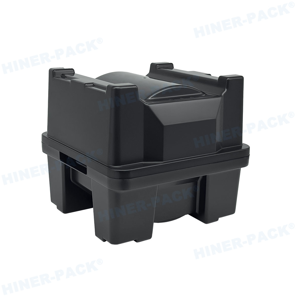
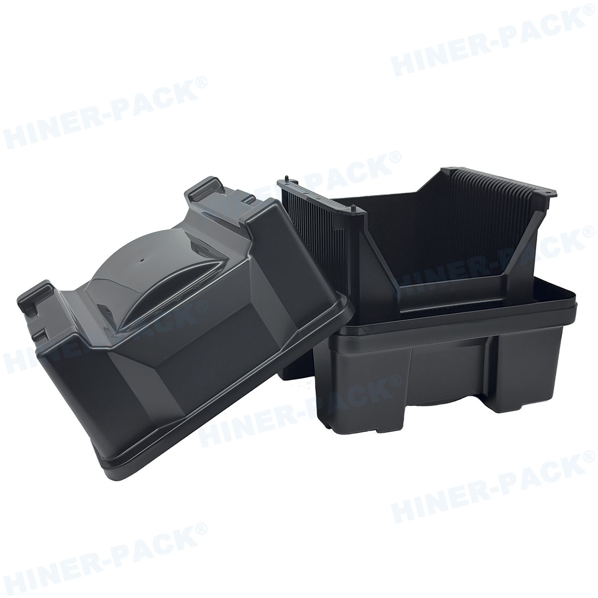
A semiconductor cassette is a specialized container designed to hold multiple silicon wafers in a secure, organized manner during various stages of semiconductor manufacturing. Typically made from materials like polycarbonate or stainless steel, these cassettes feature slots that keep wafers separated and aligned, preventing contact that could lead to scratches or breakage. The standard semiconductor cassette can accommodate wafers of different sizes, such as 200mm, 300mm, or even larger diameters, and is engineered to meet strict cleanliness standards, often complying with ISO Class 1 cleanroom requirements. The primary function of a semiconductor cassette is to facilitate safe storage and transport within a fabrication facility, but it also integrates with automated systems for efficient semiconductor wafer handling.
The evolution of the semiconductor cassette has been driven by the increasing complexity of semiconductor devices. In early days, simple plastic carriers sufficed, but today's cassettes are equipped with features like RFID tags for tracking, ventilation holes to minimize particle accumulation, and ergonomic designs for easy robotic manipulation. A key aspect of semiconductor cassette design is compatibility with semiconductor wafer boxes, which are often used for longer-term storage or shipping. While the terms "cassette" and "box" are sometimes used synonymously, cassettes are generally more focused on in-fab mobility, whereas boxes might offer enhanced protection for external transport. Understanding the semiconductor cassette is the first step toward grasping the broader ecosystem, including semiconductor wafer carrier systems and semiconductor wafer shipping protocols. In essence, the semiconductor cassette acts as the linchpin in wafer logistics, ensuring that these delicate substrates remain pristine from production to packaging.
The Role of Semiconductor Wafer Boxes
Semiconductor wafer boxes are essential complements to semiconductor cassette units, providing robust enclosures for wafers when they are not actively being processed. These boxes, also known as wafer pods or containers, are designed to shield wafers from environmental hazards such as dust, moisture, and static electricity. Unlike standard semiconductor cassette designs that are optimized for frequent access, semiconductor wafer boxes often feature sealed lids and desiccant packs to maintain a controlled atmosphere, making them ideal for storage or semiconductor wafer shipping. Common types include Front-Opening Unified Pods (FOUPs) for 300mm wafers and Standard Mechanical Interface (SMIF) pods for smaller wafers, both of which integrate seamlessly with semiconductor wafer handling automation.
The importance of semiconductor wafer boxes in the supply chain cannot be overlooked. They serve as the primary interface between semiconductor cassette systems and external logistics, ensuring that wafers are protected during transitions between facilities. For instance, when wafers are moved from a fab to an assembly plant, semiconductor wafer boxes provide the necessary rigidity and contamination control. Materials used in these boxes are carefully selected to minimize outgassing and particle generation, with advanced models incorporating sensors for real-time monitoring of temperature and humidity. This synergy between semiconductor cassette and semiconductor wafer boxes highlights the need for standardized designs to avoid compatibility issues. In practice, a typical workflow might involve transferring wafers from a semiconductor cassette to a semiconductor wafer box for safe shipping, underscoring the interconnected nature of these components. By optimizing semiconductor wafer boxes, manufacturers can reduce yield loss and enhance overall efficiency in semiconductor wafer handling and semiconductor wafer shipping processes.
Best Practices in Semiconductor Wafer Handling
Semiconductor wafer handling refers to the procedures and equipment used to transport wafers between process tools, storage units, and inspection stations without causing damage. This process is intrinsically linked to the semiconductor cassette, as cassettes are the primary vessels used during handling. Effective semiconductor wafer handling requires a combination of automated systems, manual protocols, and environmental controls to minimize risks like contamination, misalignment, or breakage. Robotic arms are commonly employed in modern fabs to pick wafers from a semiconductor cassette and place them into processing equipment, ensuring precision and speed. However, even with automation, proper training is essential for personnel involved in semiconductor wafer handling to handle exceptions or manual interventions safely.
Key best practices in semiconductor wafer handling include maintaining cleanroom standards, using certified handling tools, and implementing regular audits. For example, wafers should always be handled in ISO Class 3 or better environments to prevent particulate contamination. When transferring wafers from a semiconductor cassette to a tool, operators must avoid sudden movements that could cause wafer slippage. Additionally, semiconductor wafer handling protocols often involve the use of semiconductor wafer carrier systems that provide additional stability during movement. Another critical aspect is the integration of semiconductor wafer boxes for intermediate storage, which helps buffer wafers between handling steps. Common challenges in semiconductor wafer handling include electrostatic discharge (ESD) and mechanical stress, which can be mitigated through grounded equipment and cushioned cassette designs. By adhering to these practices, companies can improve throughput and reduce defects, making semiconductor wafer handling a cornerstone of efficient fab operations. The role of the semiconductor cassette here is pivotal, as its design directly influences handling efficiency—for instance, cassettes with wider slots may ease robotic pickup but risk less secure holding.
Types of Semiconductor Wafer Carriers
Semiconductor wafer carrier is a broad term that encompasses various devices used to hold and transport wafers, including semiconductor cassette units and semiconductor wafer boxes. These carriers are categorized based on their application, wafer size, and level of automation. The most common types include open cassettes, closed pods, and specialized carriers for specific processes. Open cassettes, often synonymous with basic semiconductor cassette designs, are used for short-distance moves within a cleanroom and allow easy access to wafers. In contrast, closed pods like FOUPs (Front-Opening Unified Pods) provide a sealed environment, making them suitable for semiconductor wafer shipping and long-term storage. Another variant is the FOSB (Front-Opening Shipping Box), which is optimized for inter-facility transport and integrates with both semiconductor cassette systems and semiconductor wafer handling equipment.
The evolution of semiconductor wafer carrier technology has been driven by the shift toward larger wafer sizes and higher automation. For 300mm wafers, FOUPs have become the standard, featuring front-opening doors that interface directly with tool loadports. This design minimizes exposure to contaminants and supports high-speed semiconductor wafer handling. Similarly, SMIF (Standard Mechanical Interface) pods are used for smaller wafers and offer a compact, scalable solution. The choice of semiconductor wafer carrier depends on factors such as the required level of protection, compatibility with existing semiconductor cassette infrastructure, and cost considerations. For example, in high-volume fabs, investing in advanced semiconductor wafer carrier systems can yield significant returns by reducing downtime and improving yield. However, this also introduces complexities in semiconductor wafer shipping, as carriers must be durable enough to withstand logistics hazards. Understanding the types of semiconductor wafer carrier options available helps manufacturers select the right solution for their needs, ensuring seamless integration with semiconductor wafer boxes and handling protocols.
Semiconductor Wafer Shipping: Methods and Considerations
Semiconductor wafer shipping involves the transportation of wafers between different locations, such as from a fab to a testing facility or an overseas customer. This process requires meticulous planning to protect the delicate wafers from physical shock, temperature fluctuations, and contamination. The semiconductor cassette plays a central role here, as wafers are typically shipped while housed in cassettes or within more robust semiconductor wafer boxes. Semiconductor wafer shipping methods range by air, land, or sea, each with its own set of challenges. Air freight is fastest but exposes wafers to pressure changes, while sea freight is cost-effective but involves longer transit times and higher humidity risks. Regardless of the mode, semiconductor wafer shipping must adhere to international standards, such as those set by SEMI (Semiconductor Equipment and Materials International), to ensure consistency.
Key considerations in semiconductor wafer shipping include packaging, tracking, and insurance. Packaging often involves multiple layers: wafers in a semiconductor cassette are placed inside a semiconductor wafer box, which is then secured in a shock-absorbent outer container with desiccants and humidity indicators. This layered approach mitigates risks during semiconductor wafer handling in transit. Additionally, real-time tracking systems using GPS or IoT sensors are becoming common, allowing stakeholders to monitor conditions like temperature and vibration. Another critical aspect is customs compliance, as wafers are high-value items subject to export controls. The interplay between semiconductor wafer shipping and semiconductor wafer carrier design is evident—carriers must be stackable and space-efficient to optimize shipping costs. Common problems in semiconductor wafer shipping include delays, mishandling, and environmental breaches, which can lead to costly rejects. By implementing best practices, such as using certified semiconductor wafer boxes and partnering with experienced logistics providers, companies can minimize these risks. The semiconductor cassette, as the innermost protector, must be designed to withstand shipping stresses, highlighting the need for durable materials and secure latching mechanisms.
Common Problems in Semiconductor Cassette Systems
Despite advancements, semiconductor cassette systems are prone to various issues that can compromise wafer integrity. One of the most frequent problems is contamination, which can originate from cassette materials, handling errors, or environmental factors. Particles generated within a semiconductor cassette can adhere to wafer surfaces, causing defects in subsequent processing steps. This is often exacerbated by poor cleaning protocols or incompatible semiconductor wafer boxes. Another common issue is mechanical damage, such as wafer chipping or breakage due to misalignment in cassette slots. This can occur during semiconductor wafer handling if cassettes are overfilled or if robotic systems are miscalibrated. Additionally, semiconductor cassette designs may suffer from wear and tear over time, leading to issues like slot deformation or latch failures, which become critical during semiconductor wafer shipping.
Electrostatic discharge (ESD) is another significant problem in semiconductor cassette systems. Wafers are highly sensitive to ESD, which can damage circuits even before they are fully fabricated. Cassettes made from non-conductive materials can accumulate static charge, especially in low-humidity environments. This risk extends to semiconductor wafer carrier units and semiconductor wafer handling equipment, requiring comprehensive grounding strategies. Furthermore, compatibility issues between different semiconductor cassette types and semiconductor wafer boxes can cause misalignment or jamming during automated transfers. For example, a cassette designed for one brand of tool may not fit properly into another, disrupting the workflow. In semiconductor wafer shipping, problems like shock damage or temperature excursions are common if cassettes and boxes are not adequately insulated. To address these, regular maintenance, material upgrades, and standardization are essential. By identifying these common problems early, manufacturers can implement preventive measures, such as using antistatic cassettes or conducting routine inspections, to safeguard their wafers throughout the lifecycle.
Solutions and Best Practices for Optimal Performance
Addressing the challenges in semiconductor cassette systems requires a multifaceted approach that integrates technology, training, and standardization. For contamination control, solutions include using high-purity materials for cassettes and implementing rigorous cleaning cycles. Automated wafer cleaners can be employed to sanitize semiconductor cassette units between uses, reducing particle counts. Additionally, adopting closed semiconductor wafer carrier systems like FOUPs can minimize exposure during semiconductor wafer handling. To prevent mechanical damage, manufacturers should invest in precision-engineered cassettes with reinforced slots and conduct regular calibration of handling robots. Training programs for personnel on proper semiconductor wafer handling techniques are also crucial, emphasizing gentle movements and correct loading procedures.
For ESD mitigation, conductive or dissipative materials should be used in semiconductor cassette construction. Grounding straps and ionizers can be installed in handling areas to neutralize static charges. Compatibility issues can be resolved by adhering to industry standards, such as SEMI specifications for cassette dimensions, which ensure interoperability between different semiconductor wafer boxes and tools. In semiconductor wafer shipping, solutions involve using advanced packaging materials with cushioning and climate control, as well as partnering with logistics providers specializing in high-value goods. Real-time monitoring during transit allows for quick response to environmental changes. Best practices also include preventive maintenance schedules for semiconductor cassette inventory, replacing worn units before they fail. By leveraging these solutions, companies can enhance the reliability of their semiconductor cassette systems, improve semiconductor wafer handling efficiency, and reduce costs associated with wafer loss. Ultimately, a proactive stance on problem-solving ensures that the entire ecosystem—from cassette to shipping—operates seamlessly.
Future Trends in Semiconductor Cassette Technology
The future of semiconductor cassette technology is shaped by trends like miniaturization, automation, and sustainability. As wafer sizes increase and feature sizes shrink, cassettes must evolve to support higher densities and stricter cleanliness requirements. Smart semiconductor cassette systems embedded with sensors for real-time monitoring of parameters like temperature, humidity, and vibration are gaining traction. These IoT-enabled cassettes can communicate with semiconductor wafer handling systems to optimize workflows and predict maintenance needs. Additionally, advancements in materials science may lead to cassettes made from recyclable or low-outgassing polymers, reducing environmental impact and improving compatibility with semiconductor wafer boxes.
Another trend is the integration of AI and machine learning into semiconductor wafer handling processes. AI algorithms can analyze data from cassettes to identify patterns in contamination or damage, enabling predictive adjustments. In semiconductor wafer shipping, blockchain technology might be used for secure tracking and authentication, enhancing supply chain transparency. The role of the semiconductor wafer carrier is also evolving, with designs focusing on lightweight yet durable constructs to lower shipping costs. As the industry moves toward more sustainable practices, we may see reusable semiconductor cassette systems that minimize waste. These innovations will not only address current problems but also open new possibilities for efficiency and reliability. By staying abreast of these trends, manufacturers can future-proof their operations and maintain a competitive edge.
In summary, the semiconductor cassette is a critical component in the semiconductor industry, serving as the foundation for safe wafer management. Its interplay with semiconductor wafer boxes, semiconductor wafer handling protocols, semiconductor wafer carrier designs, and semiconductor wafer shipping logistics forms a complex but essential system. Throughout this article, we have explored the functions, challenges, and solutions associated with these elements, emphasizing the importance of standardization and best practices. Common problems like contamination and mechanical damage can be mitigated through proactive measures, ensuring high yield and operational efficiency. As technology advances, the semiconductor cassette will continue to evolve, incorporating smart features and sustainable materials. By understanding and optimizing this ecosystem, stakeholders can enhance productivity and drive innovation in semiconductor manufacturing. Whether you are involved in design, production, or logistics, a deep knowledge of semiconductor cassette systems is invaluable for success in this dynamicfield.


