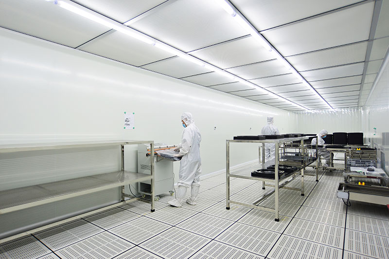
In the highly precise world of semiconductor manufacturing, every component plays a critical role in ensuring the integrity and yield of the final product. Among the most vital components in the front-end processes is the EPAK wafer carrier. This seemingly simple container is, in fact, a masterpiece of engineering designed to protect valuable silicon wafers from contamination, physical damage, and environmental fluctuations. This article delves deep into the EPAK wafer carrier, exploring its fundamental aspects, design intricacies, and the common challenges associated with its use. Understanding this essential tool is key to optimizing semiconductor production lines.
What is an EPAK Wafer Carrier and Why is it Crucial?
An EPAK wafer carrier, often referred to simply as a FOUP (Front-Opening Unified Pod), is a standardized enclosure used to store and transport silicon wafers between tools in an automated semiconductor fabrication plant (fab). The "front-opening" design is a key differentiator, allowing robotic arms to access wafers from a single, standardized plane. The primary mission of the EPAK wafer carrier is to act as a mini-cleanroom, creating a controlled microenvironment that shields wafers from airborne molecular contaminants (AMC), particles, and humidity. Without the protection offered by a reliable EPAK wafer carrier, multi-million dollar wafer batches would be susceptible to defects, leading to catastrophic yield losses.
The Material Science Behind the EPAK Wafer Carrier
The choice of material for an EPAK wafer carrier is not arbitrary; it is a careful balance of properties essential for cleanroom compatibility and durability.
Polycarbonate and PPS (Polyphenylene Sulfide): Most modern EPAK wafer carriers are manufactured from advanced, static-dissipative polymers like polycarbonate or PPS. These materials are selected for their exceptional purity, low outgassing properties, and high mechanical strength.
Low Outgassing: In the vacuum of certain process tools, materials can release trapped gases (outgassing), which can contaminate chamber interiors and deposit on wafer surfaces. The polymers used in an EPAK wafer carrier are engineered to minimize this risk.
Static Control: The buildup of static electricity can attract airborne particles like a magnet. Static-dissipative materials prevent this charge accumulation, a critical feature for maintaining wafer cleanliness inside the EPAK wafer carrier.
Chemical Resistance: The carrier must withstand frequent cleaning with aggressive chemicals without degrading, warping, or becoming a source of contamination itself.
Key Design Features of a Modern EPAK Wafer Carrier
The effectiveness of an EPAK wafer carrier lies in its sophisticated design elements, each serving a specific purpose.
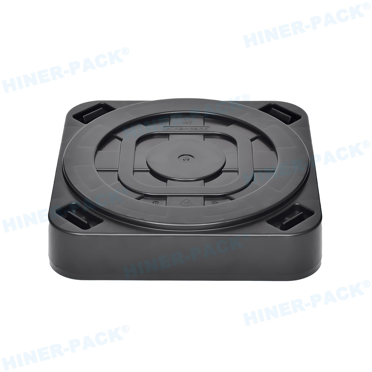
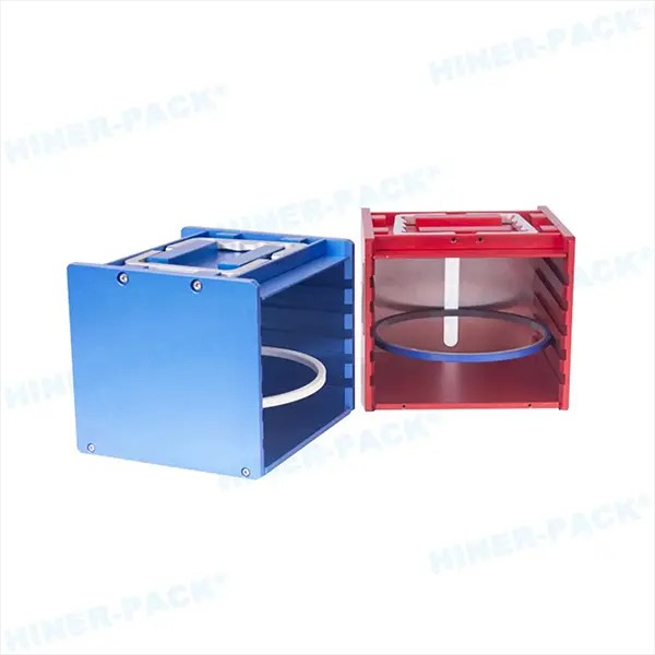
Precision Wafer Slots: The interior of the carrier contains precisely molded slots that cradle each wafer individually. These slots are designed to minimize contact points, reducing the risk of backside particles and physical stress on the wafer.
RFID Tag Integration: A modern EPAK wafer carrier is typically equipped with a radio-frequency identification (RFID) tag. This tag stores vital information about the wafers inside, such as wafer lot ID, process history, and recipe data, enabling seamless tracking and automation throughout the fab.
Kinematic Coupling Mounts: The bottom of the carrier features kinematic mounts. These ensure highly repeatable and precise positioning when the EPAK wafer carrier is placed on a process tool or transport system. This accuracy is fundamental for the robotic arm to correctly access every wafer slot.
Door Latching Mechanism: The door features a robust yet precise latching system that ensures a perfect seal when closed. This mechanism must engage smoothly and reliably thousands of times over the carrier's lifespan to maintain the protective environment.
Different Types and Capacities of EPAK Wafer Carriers
The EPAK wafer carrier is not a one-size-fits-all solution. It is designed to accommodate different wafer sizes and production needs.
Wafer Size Compatibility: While the standard has evolved over time, EPAK wafer carriers are primarily designed for 300mm wafers, which is the current mainstream standard for high-volume semiconductor manufacturing. The design principles also apply to carriers for newer, larger formats.
Capacity Variations: A standard 300mm EPAK wafer carrier typically holds 25 wafers. However, different capacities are available (e.g., 13-wafer carriers) to suit specific process requirements or tool configurations.
The Manufacturing and Maintenance Lifecycle
The journey of an EPAK wafer carrier involves rigorous manufacturing and a strict maintenance regimen to ensure ongoing performance.
High-Precision Molding: Manufacturing involves injection molding with ultra-precise molds to achieve the required dimensional tolerances. Post-molding, each carrier undergoes thorough inspection and cleaning.
Cleaning and Re-certification: After being used in the fab, an EPAK wafer carrier must be cleaned to remove any accumulated particles or films. This is done in specialized wafer carrier cleaning machines. Following cleaning, the carrier is tested and re-certified to meet strict cleanliness standards before being released back into production.
Periodic Maintenance: Over time, components like the door seal and latching mechanism may wear out. A comprehensive maintenance program includes replacing these consumable parts to extend the service life of the EPAK wafer carrier.
Common Questions and Challenges with EPAK Wafer Carriers
Even with robust design, users of the EPAK wafer carrier can encounter several common issues.
1. Particle Generation and Contamination
This is the most significant challenge. Particles can originate from several sources:
Wear and Tear: Mechanical contact between the wafer and the carrier slots, or the door latching process, can generate microscopic particles over time.
Improper Handling: Manual mishandling can cause scratches or cracks on the carrier's interior, creating particle generation sites.
Ineffective Cleaning: If the cleaning process is not performed correctly or frequently enough, contaminants can accumulate.
2. Outgassing Issues
If an EPAK wafer carrier is made from sub-standard material or has been exposed to excessive heat or chemicals, it may begin to outgas. These vapors can condense on wafers inside the carrier or within a process tool, leading to defects.
3. Mechanical Failures
The door latching mechanism is a common point of failure. A misaligned or worn-out latch can prevent a proper seal, compromising the internal environment. Similarly, damage to the kinematic mounts can lead to misalignment on tools, causing robotic handling errors.
4. Electrostatic Discharge (ESD) Risks
If the static-dissipative properties of the EPAK wafer carrier material degrade, it can lead to ESD events. These discharges can damage the delicate circuits on the wafers.
5. Moisture Control
In some processes, controlling humidity within the carrier microenvironment is critical. A compromised seal or the use of a material that absorbs moisture can lead to problems like wafer oxidation or hazing.
The EPAK wafer carrier is far more than a simple box. It is a highly engineered, critical component that safeguards the heart of the semiconductor industry—the silicon wafer. From its material composition to its intelligent design features, every aspect of the EPAK wafer carrier is optimized for protection, automation, and cleanliness. By understanding its functions and being proactive about the common challenges like particle control and mechanical maintenance, fabrication facilities can maximize wafer yield, reduce downtime, and ensure the smooth flow of production. The reliability of the entire manufacturing process often hinges on the humble, yet indispensable, EPAK wafer carrier.