
Imagine a world where the tiny chips powering our devices are mishandled, leading to costly failures and production delays. At the heart of semiconductor manufacturing lies a crucial, often overlooked tool: the silicon wafer carrier. This essential device ensures that delicate silicon wafers—the building blocks of electronics—are transported, stored, and processed with precision and care. In an industry where even microscopic contaminants can ruin entire batches, the role of the silicon wafer carrier cannot be overstated. From safeguarding multi-million-dollar production lines to enabling advancements in technology, these carriers are the unsung heroes of the electronics world. In this article, we delve into the intricacies of silicon wafer carriers, exploring their design, materials, and impact on modern manufacturing. Whether you're an engineer, a tech enthusiast, or simply curious about how our gadgets are made, understanding the silicon wafer carrier provides valuable insights into the backbone of innovation.
What is a Silicon Wafer Carrier?
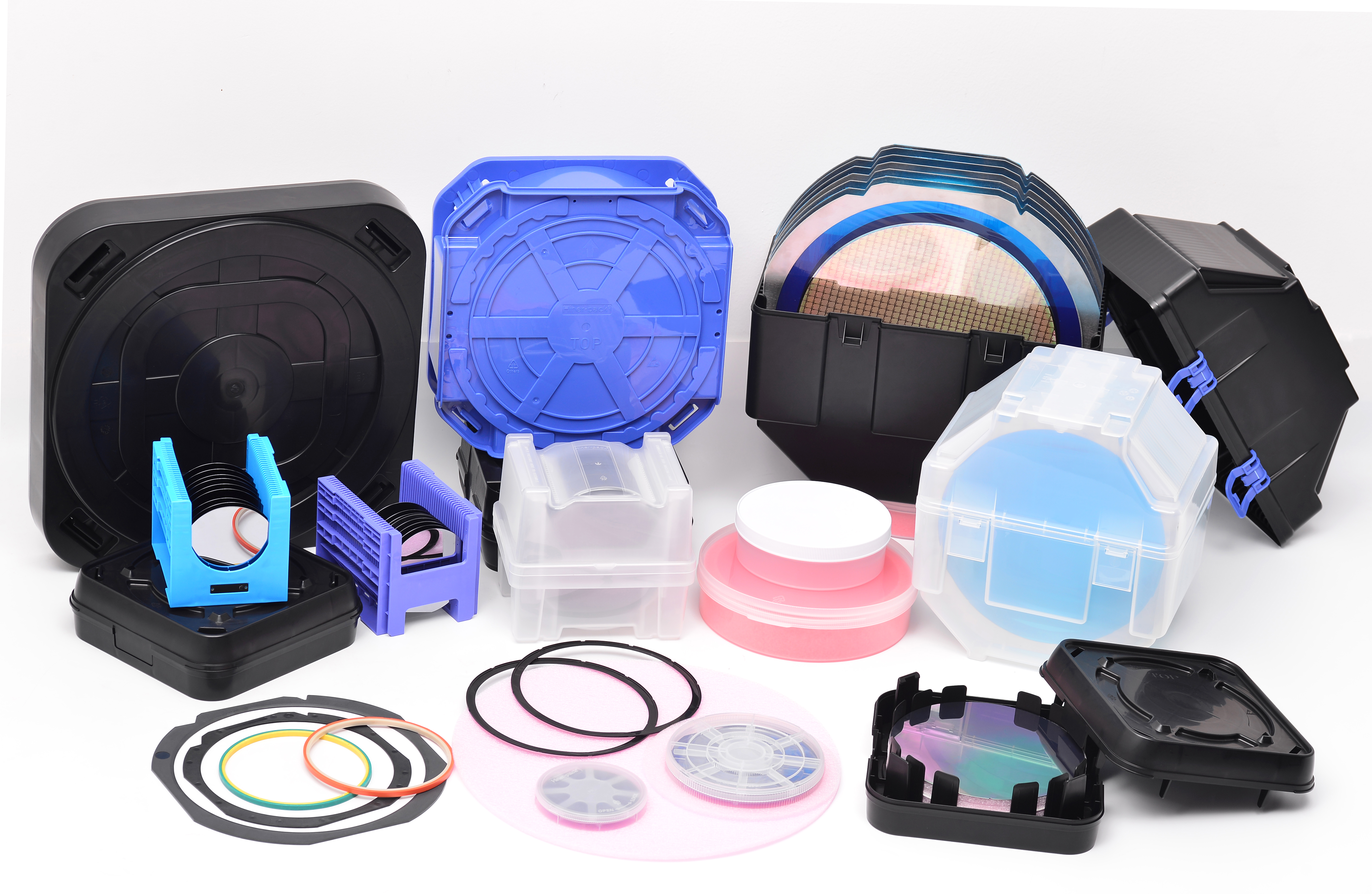
A silicon wafer carrier is a specialized container designed to hold and protect silicon wafers during various stages of semiconductor fabrication. These wafers, typically thin discs of silicon, form the substrate for integrated circuits and other microdevices. The primary purpose of a silicon wafer carrier is to prevent damage, contamination, and electrostatic discharge, which could compromise the wafers' integrity. Typically made from high-purity materials, these carriers feature slots or grooves that securely cradle each wafer, allowing for safe handling in cleanroom environments. The design of a silicon wafer carrier must adhere to strict industry standards to ensure compatibility with automated equipment, such as robotic arms and processing tools. As semiconductor technology advances, with wafers growing larger and features shrinking, the silicon wafer carrier evolves to meet these demands, emphasizing precision and reliability. Without a robust silicon wafer carrier, the entire manufacturing process would be prone to errors, leading to increased costs and reduced yields. Thus, this component is indispensable in maintaining the high-quality standards required in electronics production.
Types and Designs of Silicon Wafer Carriers
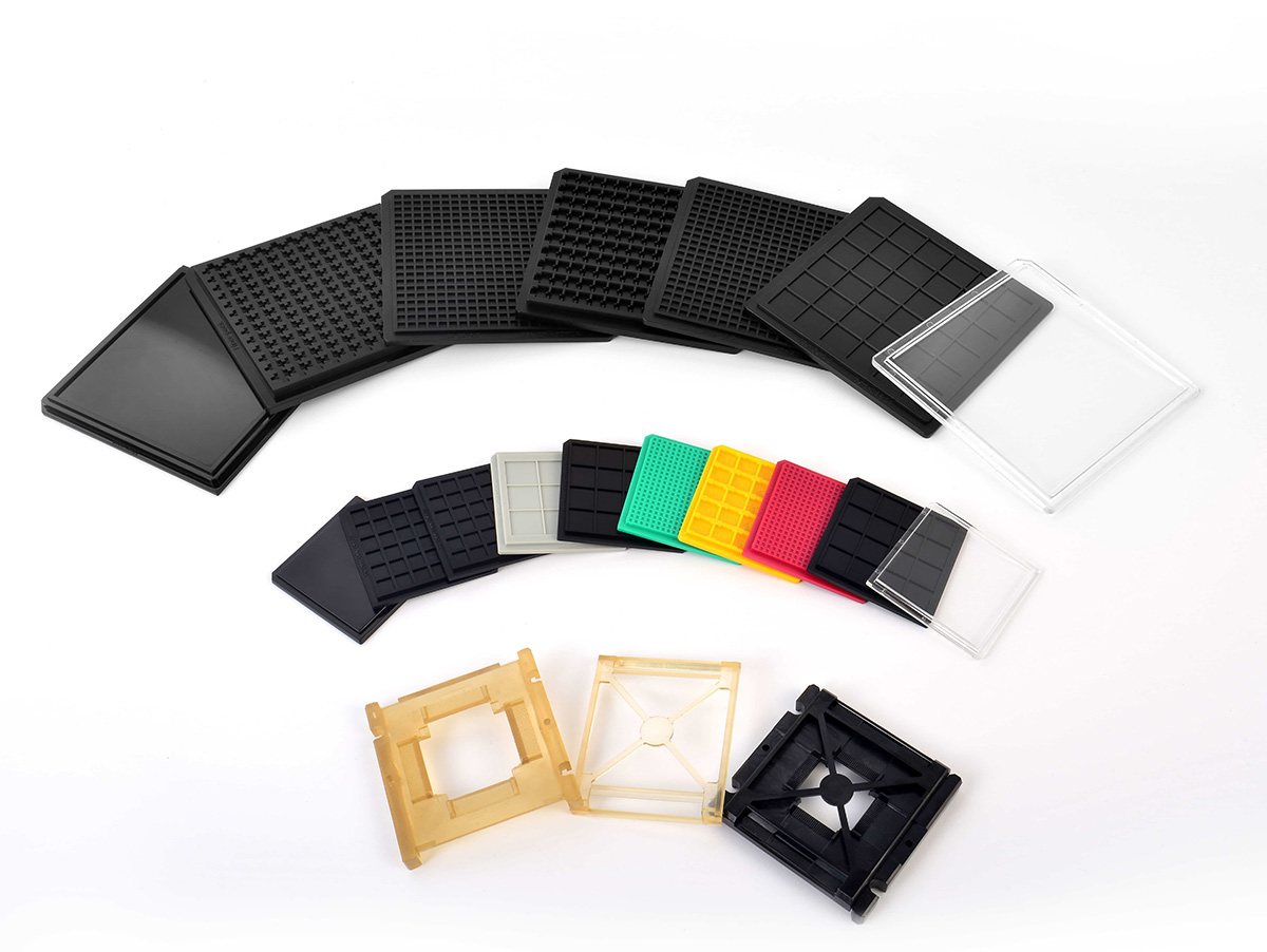
Silicon wafer carriers come in various types and designs, each tailored to specific applications and wafer sizes. Common variants include front-opening unified pods (FOUPs), standard mechanical interface (SMIF) pods, and cassette-style carriers. FOUPs, for instance, are widely used in advanced fabrication facilities for 300mm wafers, featuring a front-opening mechanism that minimizes contamination during loading and unloading. SMIF pods, on the other hand, are often employed for smaller wafers and provide an isolated environment to protect against particles. Cassette carriers are simpler in design, typically holding multiple wafers in a horizontal or vertical orientation for transport between process steps. The design of a silicon wafer carrier incorporates elements like handles, locking mechanisms, and identification features (e.g., RFID tags or barcodes) to facilitate automation and tracking. Materials and structural integrity are optimized to withstand harsh conditions, such as high temperatures and chemical exposures, common in semiconductor processing. Innovations in silicon wafer carrier design continue to emerge, focusing on reducing weight, enhancing durability, and improving ergonomics for handlers. By selecting the appropriate type of silicon wafer carrier, manufacturers can streamline operations and boost efficiency in their production lines.
Materials Used in Silicon Wafer Carriers
The materials chosen for a silicon wafer carrier are critical to its performance, as they must ensure minimal contamination, high strength, and resistance to environmental factors. Common materials include high-purity plastics like polycarbonate, PEEK (polyether ether ketone), and PTFE (polytetrafluoroethylene), which offer excellent chemical resistance and low particle generation. For more demanding applications, carriers may incorporate metals such as stainless steel or aluminum, often anodized or coated to prevent corrosion and static buildup. The selection process for silicon wafer carrier materials involves rigorous testing to meet industry standards, such as those set by SEMI (Semiconductor Equipment and Materials International). Factors like thermal stability, electrical conductivity, and cleanability play a key role in material choice, especially as wafers become more sensitive to defects. Additionally, sustainable materials are gaining attention, with efforts to develop recyclable or reusable silicon wafer carrier options to reduce environmental impact. By understanding the material properties, users can ensure their silicon wafer carrier maintains wafer integrity throughout the manufacturing lifecycle, ultimately contributing to higher yield rates and cost savings.
The Role of Silicon Wafer Carriers in Semiconductor Manufacturing
In semiconductor manufacturing, the silicon wafer carrier plays a pivotal role in ensuring smooth and efficient operations. From the initial wafer slicing to final packaging, these carriers protect wafers from physical damage, dust, and electrostatic discharge, which are common threats in production environments. They enable seamless integration with automated systems, allowing for high-throughput processing without manual intervention. For example, in lithography or etching steps, a silicon wafer carrier securely positions wafers for precise alignment, reducing the risk of misprocessing. Moreover, carriers facilitate inventory management and traceability through embedded identifiers, helping manufacturers monitor wafer history and comply with quality control protocols. The reliability of a silicon wafer carrier directly impacts overall equipment effectiveness (OEE), as any failure can lead to downtime and scrap. In large-scale fabs, optimizing the use of silicon wafer carriers through standardized designs and maintenance routines is essential for maximizing productivity. As the industry moves toward larger wafer diameters and more complex geometries, the silicon wafer carrier must adapt to support these advancements, underscoring its importance in the semiconductor ecosystem.
Maintenance and Handling of Silicon Wafer Carriers
Proper maintenance and handling of a silicon wafer carrier are essential to prolong its lifespan and ensure consistent performance. Regular cleaning procedures, often using ultra-pure water, solvents, or specialized detergents, help remove contaminants like particles, residues, and microbes. It's crucial to follow manufacturer guidelines and industry standards to avoid damaging the carrier's surfaces or slots. Handling should occur in controlled environments, such as cleanrooms, with operators wearing appropriate attire to minimize contamination risks. Inspection routines, including visual checks and automated scanning, can detect wear and tear, such as cracks or deformities, that might compromise wafer safety. For a silicon wafer carrier, preventive maintenance schedules should include checks for electrostatic properties and mechanical integrity. Storage conditions also matter; carriers should be kept in dry, clean areas to prevent degradation. By implementing best practices for silicon wafer carrier care, companies can reduce replacement costs and maintain high wafer yields, ultimately supporting sustainable manufacturing processes.
Future Trends in Silicon Wafer Carrier Technology
The future of silicon wafer carrier technology is shaped by emerging trends in semiconductor manufacturing, such as the adoption of larger 450mm wafers, increased automation, and sustainability initiatives. Innovations focus on enhancing carrier intelligence through IoT (Internet of Things) integration, allowing real-time monitoring of conditions like temperature and humidity. Smart silicon wafer carriers equipped with sensors could provide data analytics to predict maintenance needs and optimize workflows. Additionally, advancements in materials science may lead to lighter, stronger composites that reduce energy consumption during transport. Environmental concerns are driving the development of eco-friendly silicon wafer carrier designs, including reusable models and biodegradable materials. As the industry embraces concepts like Industry 4.0, the silicon wafer carrier will evolve into a more interconnected component, supporting digital twins and AI-driven optimization. These trends promise to make the silicon wafer carrier not just a passive container, but an active contributor to efficient and green manufacturing ecosystems.
In summary, the silicon wafer carrier is a fundamental element in semiconductor manufacturing, offering protection, efficiency, and reliability across various stages of production. From its diverse designs and material compositions to its critical role in automation and maintenance, this component ensures that silicon wafers remain pristine and functional. As technology progresses, the silicon wafer carrier will continue to adapt, incorporating smart features and sustainable practices to meet the demands of next-generation electronics. By appreciating the nuances of the silicon wafer carrier, industry professionals can make informed decisions that enhance productivity and innovation. For anyone involved in tech manufacturing, staying updated on these developments is key to leveraging the full potential of this essential tool.
Frequently Asked Questions
Q1: What is the main purpose of a silicon wafer carrier?
A1: The main purpose of a silicon wafer carrier is to protect silicon wafers from physical damage, contamination, and electrostatic discharge during storage, transport, and processing in semiconductor manufacturing. It ensures wafers remain in optimal condition for high-yield production.
Q2: How do I choose the right type of silicon wafer carrier for my application?
A2: Choosing the right silicon wafer carrier depends on factors like wafer size (e.g., 200mm, 300mm), the specific manufacturing environment (e.g., cleanroom requirements), and compatibility with automated systems. Consider carriers designed for your wafer diameter and process needs, such as FOUPs for advanced fabs or cassettes for simpler operations.
Q3: What materials are commonly used in silicon wafer carriers, and why?
A3: Common materials for silicon wafer carriers include high-purity plastics like polycarbonate and PEEK, as well as metals like stainless steel. These materials are chosen for their low particle generation, chemical resistance, and durability, which help maintain wafer integrity in harsh semiconductor environments.
Q4: How often should a silicon wafer carrier be cleaned and maintained?
A4: A silicon wafer carrier should be cleaned regularly based on usage and contamination levels, typically after each processing cycle or as per manufacturer recommendations. Preventive maintenance, including inspections for damage and electrostatic properties, should be performed periodically to ensure reliability.
Q5: Are there any emerging technologies affecting silicon wafer carrier design?
A5: Yes, emerging technologies like IoT, AI, and sustainable materials are influencing silicon wafer carrier design. Smart carriers with sensors for real-time monitoring, lighter composites for efficiency, and eco-friendly options are becoming more prevalent, aligning with trends in automation and environmental responsibility.


