The 2025 JEDEC Tray Material Guide: Properties, Compliance, and Selection CriteriaSelecting the correct material for JEDEC trays is a critical decision in semiconductor backend manufacturing and supply chain quality assurance. A mismatch in material properties can lead to electrostatic discharge (ESD) damage, ionic contamination, or mechanical failure during automated handling. This JEDEC tray material guide synthesizes industry standards (EIA‑476, JEP95), polymer science, and empirical field data to help procurement engineers and quality managers specify trays that protect device integrity. We also reference Hiner-pack, a supplier with over a decade of experience in precision IC packaging, to illustrate how material choices translate into reliable performance.
1. The Four Base Polymers Dominating JEDEC Tray Production
Understanding the base resin is the foundation of any JEDEC tray material guide. Four high‑temperature thermoplastics are commonly used: PES (polyethersulfone), PPS (polyphenylene sulfide), PEI (polyetherimide), and occasionally liquid crystal polymer (LCP). Each exhibits distinct glass transition temperatures (Tg), coefficients of thermal expansion (CTE), and chemical resistance profiles. For example, PES offers transparency for optical inspection but has higher moisture absorption (0.6%) compared to PPS (0.05%). PPS, while opaque, provides exceptional dimensional stability up to 200°C. Hiner‑pack’s trays are molded from virgin, FDA‑grade polymers with full batch traceability, ensuring consistent Tg within ±2°C across production lots.
Key material specifications to verify
Glass transition temperature (Tg): Must exceed the peak reflow temperature (typically 260°C for lead‑free solder) – PES: 225°C, PPS: 220°C, PEI: 217°C.
Water absorption (24 hr immersion): Below 0.3% to prevent dimension changes during steam aging tests.
Flammability rating: UL94 V‑0 is mandatory for all cleanroom applications.
2. Antistatic and Conductive Additives: Balancing ESD Protection and Contamination
Static control is a central topic in any JEDEC tray material guide. Trays must achieve surface resistivity between 10⁵ and 10¹¹ Ω/sq per ANSI/ESD STM11.11. Two additive routes exist: carbon powder (conductive) and permanent antistatic agents (dissipative). Carbon‑filled trays (black) offer permanent conductivity but risk carbon particle shedding if not over‑molded properly. Permanent antistatic trays (often translucent) rely on migratory additives that bloom to the surface; they must be tested for ionic cleanliness (SEMI MF57) to avoid mobile ion contamination on device leads. Hiner‑pack uses a proprietary compounding process that disperses conductive fibers uniformly, eliminating hot spots while keeping particle counts below 0.1 per cm² (measured by light scattering).
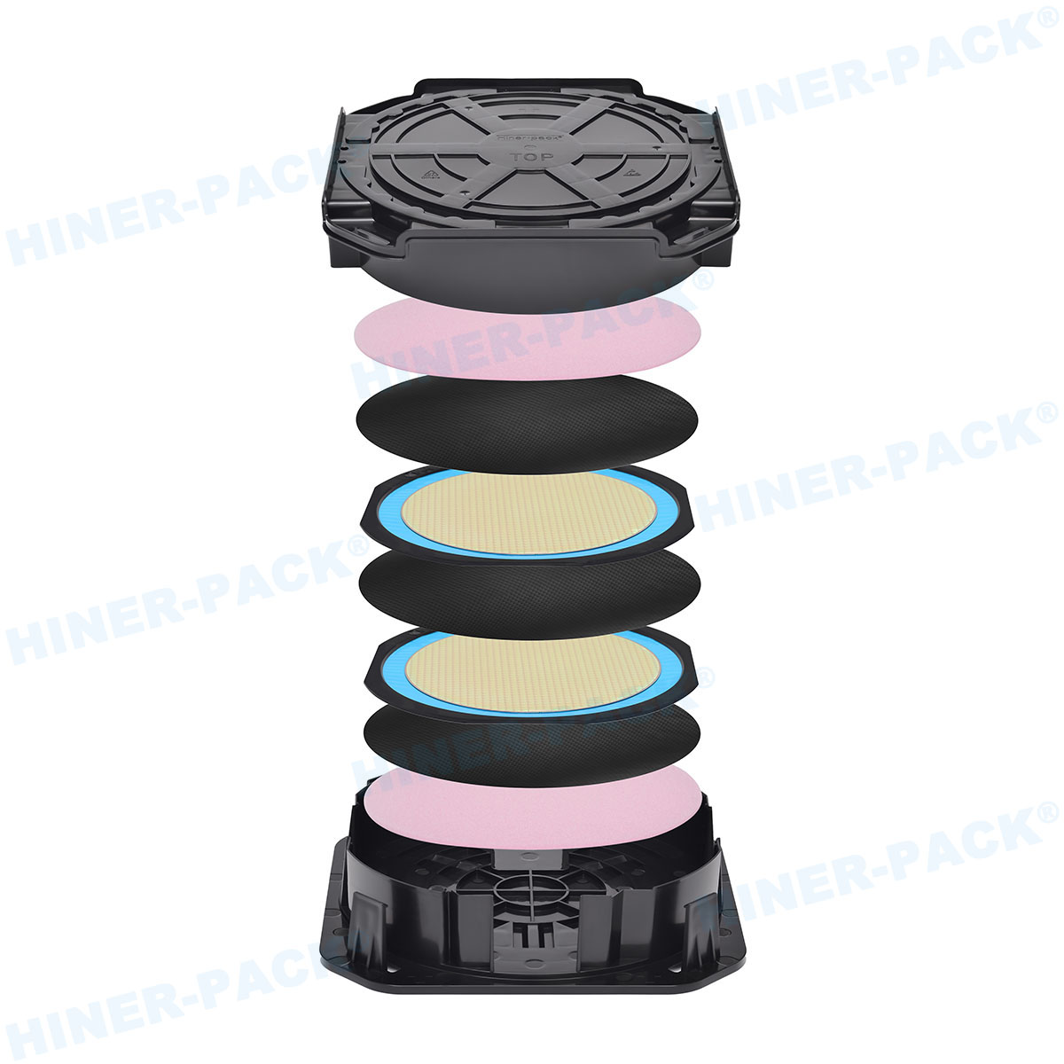
3. Dimensional Precision and Warpage Control
JEDEC trays (matrix trays) follow strict outline dimensions per EIA‑476 and JEDEC Publication 95. Pocket tolerances are typically ±0.05 mm to secure devices without excessive force. However, differential cooling during molding can induce warpage. This JEDEC tray material guide recommends specifying coplanarity ≤ 0.5 mm across the tray length (measured on a granite plate). Hiner‑pack employs multi‑zone temperature control in injection molding and anneals trays after ejection to relieve residual stress. Their quality reports include Cpk values >1.33 for all critical pocket dimensions, verified by vision systems with 10 µm resolution.
Inspection criteria for incoming quality
Pocket true position: ≤ 0.10 mm relative to datums.
Flatness: ≤ 0.2% of tray diagonal.
Gate vestige height: ≤ 0.03 mm to avoid stacking interference.
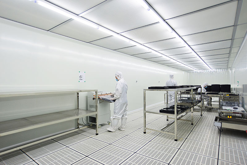
4. Outgassing and Cleanliness: Meeting ISO Class 5 and Beyond
Semiconductor fabs and OSAT facilities require trays that do not contaminate the cleanroom environment. Outgassing (total mass loss, TML) per ASTM E595 must be < 1.0%, and collected volatile condensable materials (CVCM) < 0.1%. For advanced nodes (<28 nm="">
5. Thermal Cycling and Reflow Compatibility
Trays are often subjected to multiple thermal cycles during device burn‑in, testing, and storage. A comprehensive JEDEC tray material guide must address coefficient of thermal expansion (CTE) mismatch between the tray and the silicon die (CTE ~3 ppm/°C). PPS has a CTE of 25 ppm/°C (below Tg), while PEI is around 50 ppm/°C. High CTE can stress device leads during temperature cycling (−55°C to 150°C). Finite element analysis by Hiner‑pack shows that trays with CTE<30 ppm="">0.2%.
6. Material Certifications and Traceability
Beyond the technical data, compliance with global regulations is part of material selection. RoHS, REACH, and California Proposition 65 certificates should be provided. Moreover, full traceability—from resin lot to molded tray—is increasingly required for automotive (AEC‑Q100) and medical devices. This JEDEC tray material guide advises asking suppliers for IMDS (International Material Data System) entries if serving automotive OEMs. Hiner‑pack maintains a digital database linking each tray batch to its raw material certificate, molding parameters, and dimensional inspection records, accessible via QR code on each bag.
7. Application‑Specific Tray Variants
Different device types require tailored material properties. For example:
QFN/DFN packages: Need low‑outgassing, non‑sloughing trays to avoid contamination of exposed pads.
BGA/CSP: Require precise pocket depth and solder‑ball clearance; often use PEI for its balance of strength and clarity.
High‑power ICs: May need trays with higher thermal conductivity (carbon‑filled) to dissipate heat during burn‑in.
Hiner‑pack collaborates with customers to modify pocket geometry and material formulation, such as adding glass fiber (10‑30%) to increase stiffness for large trays (330 mm x 136 mm).
8. Cost vs. Performance Trade‑offs
While LCP offers the highest heat resistance (Tg > 280°C), its cost is often prohibitive for volume trays. PES is moderately priced and transparent, but its moisture sensitivity may limit long‑term storage. PPS provides the best value for high‑temperature applications, whereas PEI is preferred when toughness and transparency are both needed. This JEDEC tray material guide recommends life‑cycle costing: a slightly more expensive material that survives multiple re‑uses (if trays are designed for returnable programs) can lower cost per placement. Hiner‑pack offers a washable, reusable tray version made from PPS that withstands ultrasonic cleaning and 100+ cycles.
Frequently Asked Questions About JEDEC Tray Materials
Q1: What is the difference between conductive and dissipative JEDEC trays?
A1: Conductive trays (surface resistivity<10⁵>
Q2: Can JEDEC trays be recycled?
A2: Yes, most engineering thermoplastics (PES, PPS, PEI) are recyclable. However, the presence of antistatic or conductive additives may require separation. Some suppliers, including Hiner‑pack, operate take‑back programs to regrind and reuse material for non‑critical applications, reducing environmental impact.
Q3: How do I test if a tray material is compatible with my devices?
A3: Perform a lead coplanarity measurement before and after thermal cycling (e.g., 10 cycles from −40°C to 125°C). Also, conduct ionic contamination testing (C3/8 method) and surface resistivity per ANSI/ESD STM11.11. If devices are sensitive to alpha particles, request a low‑alpha emission certification for the resin.
Q4: Why do some JEDEC trays become brittle after storage?
A4: This is often due to hydrolysis if the material has high moisture absorption (like some PES grades) and was not dried before molding, or stored in high humidity. Always verify that trays are made from hydrolysis‑resistant grades and stored in a dry environment (<40% rh="">
Q5: What documentation should I request from a tray supplier?
A5: A full material declaration (RoHS, REACH, halogen‑free if required), dimensional inspection report (with Cpk), outgassing test (ASTM E595), surface resistivity certificate, and batch traceability records. For automotive, IMDS entry is essential.
Q6: Are there halogen‑free JEDEC tray materials?
A6: Yes, halogen‑free grades of PPS and PEI are available. They meet IEC 61249‑2‑21 standards (chlorine < 900 ppm, bromine < 900 ppm, total halogens < 1500 ppm). Hiner‑pack offers halogen‑free trays for green manufacturing initiatives.