
Imagine a world without smartphones, computers, or advanced medical devices—it’s nearly impossible. At the heart of these technologies lies the semiconductor industry, where precision and purity are non-negotiable. One unsung hero in this intricate process is the quartz wafer carrier, a component that might seem simple but is vital for producing the chips that power our modern lives. In this article, we’ll dive deep into why quartz wafer carriers are indispensable, exploring their unique properties, applications, and more. Whether you're an engineer, a tech enthusiast, or simply curious, you'll discover how these carriers ensure the integrity of silicon wafers through every step of fabrication.
What is a Quartz Wafer Carrier?
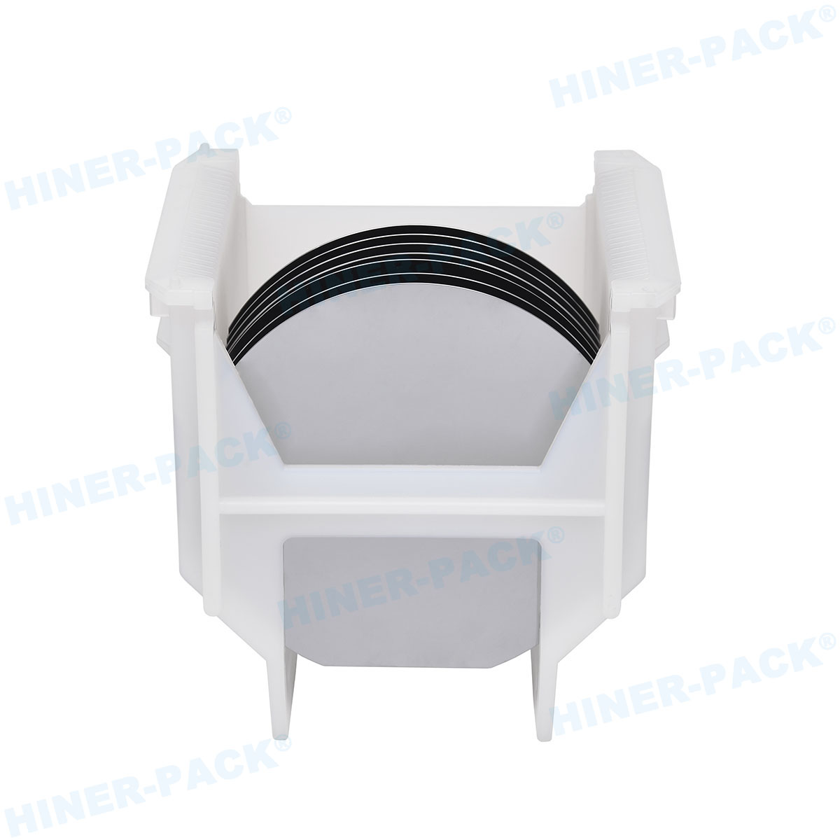
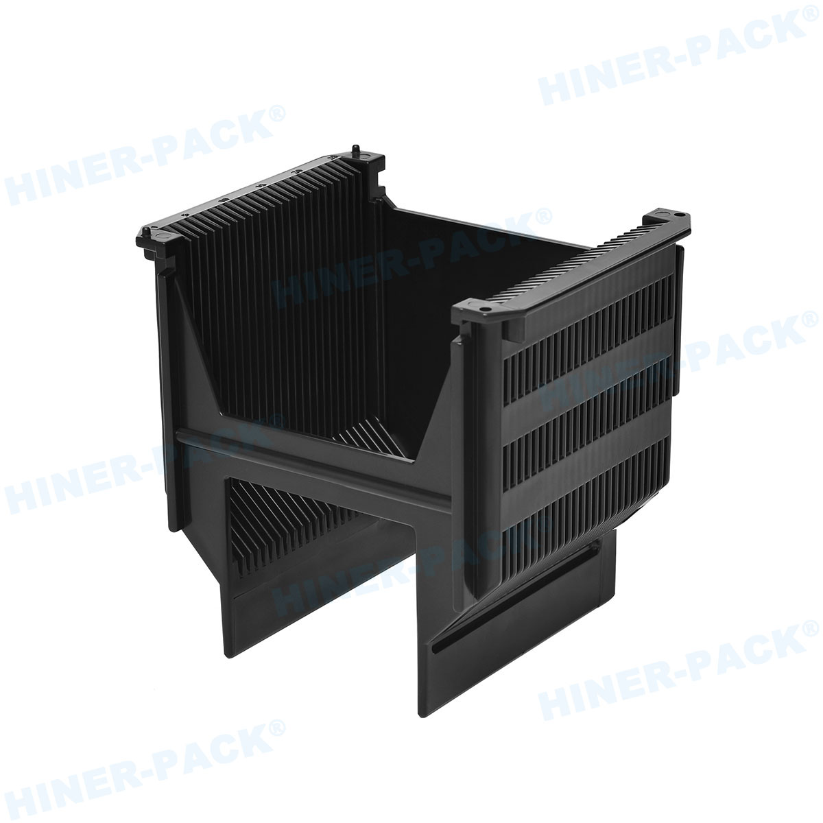
A quartz wafer carrier is a specialized holder designed to support and transport silicon wafers during semiconductor manufacturing processes. These carriers are crafted from high-purity quartz, a material chosen for its exceptional durability and resistance to extreme conditions. In cleanroom environments, where even microscopic contaminants can ruin entire batches of wafers, the quartz wafer carrier acts as a protective shield. It ensures that wafers remain stable and uncontaminated as they move through various stages, such as etching, deposition, and thermal processing. The design typically includes slots or grooves to securely hold multiple wafers, allowing for efficient handling in automated systems. Without a reliable quartz wafer carrier, the yield and quality of semiconductor devices would plummet, leading to increased costs and production delays. This makes the quartz wafer carrier a cornerstone of the electronics supply chain, underscoring its importance in high-tech manufacturing.
Key Properties of Quartz Material
The effectiveness of a quartz wafer carrier stems from the inherent properties of quartz itself. Quartz, primarily composed of silicon dioxide, offers a combination of thermal, chemical, and physical characteristics that make it ideal for semiconductor applications. First, its high thermal stability allows it to withstand temperatures exceeding 1000°C without deforming or degrading. This is crucial in processes like diffusion and annealing, where wafers are subjected to intense heat. Second, quartz exhibits excellent chemical inertness, meaning it doesn't react with aggressive chemicals used in cleaning or etching, such as acids and solvents. This prevents contamination and ensures the purity of the wafers. Additionally, quartz has low thermal expansion, reducing the risk of warping or cracking under rapid temperature changes. Its transparency to certain wavelengths of light also facilitates inspection and alignment in photolithography steps. Moreover, quartz is highly resistant to radiation and electrical interference, which is vital for maintaining performance in sensitive environments. These properties collectively make the quartz wafer carrier a reliable choice, ensuring long-term usability and minimal maintenance in demanding settings.
Applications in Semiconductor Fabrication
In semiconductor fabrication, the quartz wafer carrier plays a multifaceted role across multiple stages. During wafer cleaning, it holds wafers securely while they undergo chemical baths to remove impurities. In thermal processing, such as oxidation or doping, the carrier must endure high temperatures without releasing particles or altering the wafer's properties. For chemical vapor deposition (CVD), where thin films are applied to wafers, the quartz wafer carrier provides a stable platform that doesn't interfere with the deposition process. It's also essential in etching and lithography, where precise positioning is critical for creating intricate circuit patterns. Beyond these, quartz wafer carriers are used in testing and inspection phases, where their transparency allows for optical measurements without removing the wafers. This versatility extends to emerging fields like MEMS (Micro-Electro-Mechanical Systems) and photonics, where precision handling is paramount. By integrating seamlessly into automated production lines, the quartz wafer carrier enhances efficiency and reduces downtime, making it a key enabler of innovation in electronics and beyond.
Manufacturing Process of Quartz Wafer Carriers
The production of a quartz wafer carrier involves several meticulous steps to ensure high quality and performance. It begins with the selection of raw quartz material, which is purified to remove impurities like metals and other oxides. This purified quartz is then melted in a high-temperature furnace, often using processes like flame hydrolysis or electric fusion, to form a homogeneous glass-like substance. Next, the molten quartz is shaped into the desired carrier form through methods such as molding, machining, or precision cutting. Advanced techniques like CNC machining are employed to create precise slots and features that accommodate standard wafer sizes, such as 200mm or 300mm diameters. After shaping, the carriers undergo rigorous polishing to achieve a smooth surface, minimizing the risk of particle generation during use. Quality control steps, including visual inspection, dimensional checks, and purity testing, ensure that each quartz wafer carrier meets industry standards. Finally, annealing may be applied to relieve internal stresses, enhancing durability. This careful manufacturing process results in a product that consistently performs in critical applications, highlighting why the quartz wafer carrier is trusted in high-stakes environments.
Advantages Over Alternative Materials
When compared to carriers made from other materials like silicon carbide, plastic, or metals, the quartz wafer carrier offers distinct benefits that justify its prevalence. One major advantage is its superior purity; quartz doesn't leach ions or particles, which is essential for maintaining wafer integrity in ultra-clean environments. This contrasts with metal carriers, which might corrode or shed contaminants over time. Thermally, quartz outperforms plastics and some ceramics by handling extreme heat without degradation, whereas alternatives could melt or warp. Chemically, its inert nature means it resists attack from harsh substances, unlike polymers that might dissolve or react. Additionally, quartz wafer carriers have a longer lifespan due to their hardness and wear resistance, reducing replacement frequency and overall costs. From an environmental perspective, quartz is more sustainable as it can be recycled or reused in certain processes. However, it's important to note that quartz can be brittle, requiring careful handling to prevent breakage. Despite this, the overall benefits make the quartz wafer carrier a preferred choice for high-precision industries, balancing performance with reliability.
Maintenance and Handling Best Practices
Proper maintenance of a quartz wafer carrier is essential to maximize its lifespan and performance. Regular cleaning is crucial; this typically involves using ultra-pure water, acids, or solvents in controlled environments to remove residues without damaging the quartz. For instance, a common method is immersion in a sulfuric acid-peroxide mixture, followed by rinsing and drying in a cleanroom setting. Handling should always involve gloves and tools to avoid fingerprints or contamination, as human contact can introduce oils and particles. Storage must be in dedicated, particle-free containers to prevent scratches or impacts. Inspection for cracks, chips, or surface wear should be routine, with damaged carriers repaired or replaced promptly to avoid production issues. When transporting wafers, ensure the quartz wafer carrier is securely mounted in equipment to prevent vibration-induced damage. By adhering to these practices, users can maintain the integrity of the quartz wafer carrier, ensuring consistent results in semiconductor processes. This proactive approach not only safeguards the carrier but also supports overall manufacturing efficiency and yield.
In summary, the quartz wafer carrier is a fundamental component in semiconductor manufacturing, offering unmatched purity, thermal stability, and versatility. From its role in wafer handling to its advantages over other materials, this tool enables the precision required for modern electronics. As technology advances, the demand for reliable quartz wafer carriers will only grow, driving further innovations in their design and application. By understanding its importance and maintaining it properly, industries can continue to push the boundaries of what's possible.
Frequently Asked Questions (FAQ)
Q1: What is the primary function of a quartz wafer carrier?
A1: The primary function of a quartz wafer carrier is to hold, support, and transport silicon wafers safely during semiconductor manufacturing processes, protecting them from contamination, physical damage, and environmental factors.
Q2: How does a quartz wafer carrier compare to one made of silicon carbide?
A2: While both materials offer high thermal resistance, a quartz wafer carrier generally provides better chemical inertness and purity, reducing the risk of wafer contamination. However, silicon carbide might be more durable against mechanical stress, but quartz is often preferred for its overall balance of properties in cleanroom settings.
Q3: Can quartz wafer carriers be reused, and how are they cleaned?
A3: Yes, quartz wafer carriers can be reused multiple times with proper care. Cleaning typically involves using high-purity acids or solvents in a controlled environment to remove residues, followed by rinsing and drying to ensure no contaminants remain.
Q4: What are the common sizes for quartz wafer carriers?
A4: Quartz wafer carriers are commonly designed to accommodate standard wafer sizes, such as 150mm, 200mm, and 300mm diameters, with custom sizes available for specific applications in industries like MEMS or advanced packaging.
Q5: Why is quartz the preferred material for wafer carriers in high-temperature processes?
A5: Quartz is preferred because it maintains structural integrity at temperatures over 1000°C, has low thermal expansion to prevent warping, and doesn't emit harmful particles or gases, ensuring wafer purity and process reliability in extreme conditions.


