
Have you ever stopped to think about what keeps your smartphone, laptop, or car running smoothly? At the heart of these devices are tiny, powerful chips made from silicon wafers. But how are these delicate wafers handled without a scratch? Enter semiconductor wafer cassettes—the unsung heroes of the electronics industry. These specialized containers are crucial for transporting, storing, and processing wafers in manufacturing facilities. In this article, we dive into five key aspects of semiconductor wafer cassettes that highlight their importance, design, and impact. Whether you're an engineer, a tech enthusiast, or simply curious, you'll discover why these components are indispensable in today's digital world. Let's unravel the story behind semiconductor wafer cassettes and how they shape the technology we rely on daily.
What Are Semiconductor Wafer Cassettes?
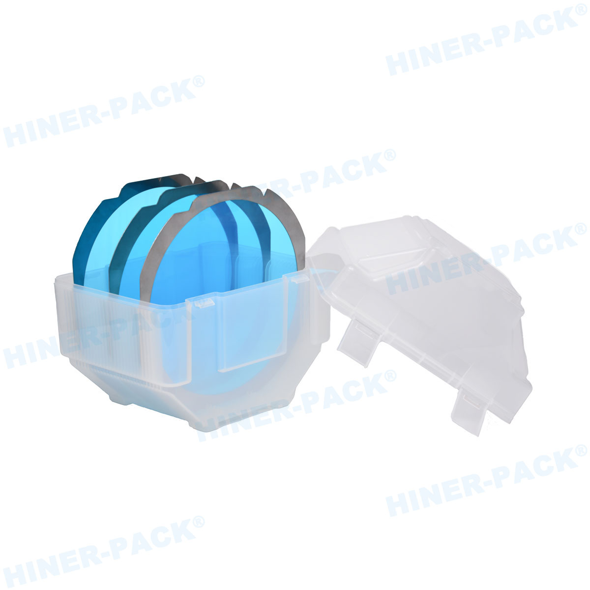
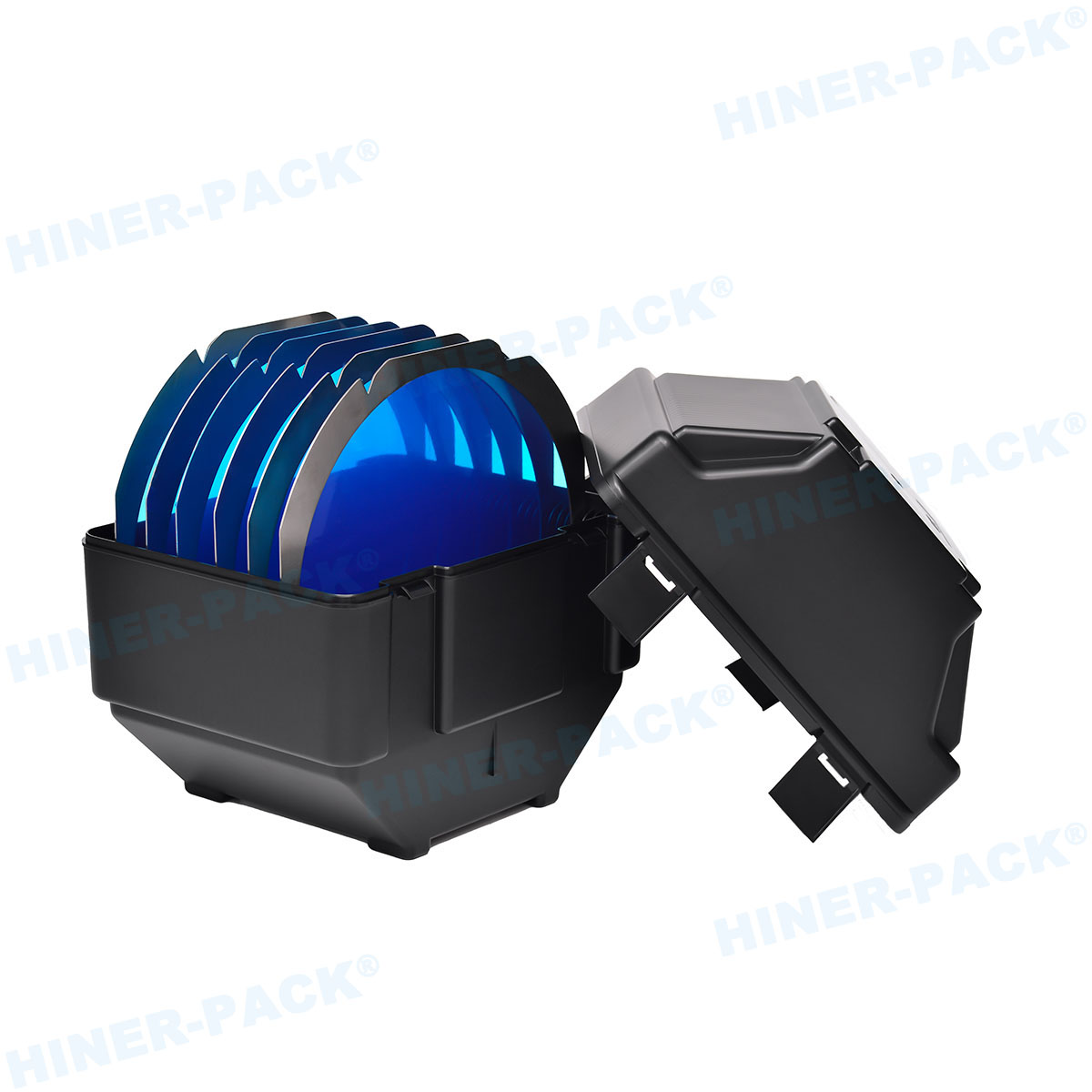
Semiconductor wafer cassettes, often referred to simply as wafer cassettes, are precision containers designed to hold and protect silicon wafers during various stages of semiconductor manufacturing. These wafers, which are thin slices of semiconductor material, form the base for integrated circuits (ICs) and microchips. The primary function of semiconductor wafer cassettes is to ensure that wafers remain contamination-free, properly aligned, and undamaged as they move through processes like etching, doping, and lithography. Typically made from high-purity materials, these cassettes feature slots that securely cradle each wafer, preventing contact and minimizing the risk of defects. In essence, semiconductor wafer cassettes act as guardians, maintaining the integrity of wafers from production to packaging. Their role is critical in achieving high yields and reliable electronic components, making them a cornerstone of the semiconductor ecosystem.
The Critical Role of Semiconductor Wafer Cassettes in Manufacturing
In the highly controlled environment of semiconductor fabrication plants (fabs), every component must meet stringent standards to avoid costly errors. Semiconductor wafer cassettes play a pivotal role here by facilitating automated handling and transport. They enable robotic systems to efficiently load and unload wafers into equipment, such as chemical vapor deposition chambers or ion implanters, without human intervention. This automation not only speeds up production but also reduces the risk of particulate contamination, which can ruin entire batches of wafers. Moreover, semiconductor wafer cassettes help in organizing wafers by lot or process step, ensuring traceability and quality control. Without these cassettes, the delicate wafers would be vulnerable to static electricity, physical stress, and environmental hazards, leading to lower productivity and increased waste. Thus, semiconductor wafer cassettes are integral to achieving the precision and scalability required in modern electronics manufacturing.
Materials and Design Innovations in Semiconductor Wafer Cassettes
The effectiveness of semiconductor wafer cassettes hinges on their materials and design, which have evolved significantly to meet industry demands. Traditionally, cassettes are fabricated from high-purity plastics like perfluoroalkoxy (PFA) or polycarbonate, chosen for their low particulate generation, chemical resistance, and static-dissipative properties. These materials prevent contamination and electrostatic discharge, which could otherwise damage sensitive wafers. In terms of design, semiconductor wafer cassettes often feature open-frame structures with precisely spaced slots to accommodate standard wafer sizes, such as 200mm, 300mm, or even emerging 450mm diameters. Advanced designs include anti-jamming mechanisms, ergonomic handles for manual handling, and RFID tags for smart tracking. Recent innovations focus on sustainability, with recyclable materials and reusable cassettes that reduce environmental impact. By continuously refining these elements, manufacturers ensure that semiconductor wafer cassettes support higher throughput and finer process nodes, aligning with the trend toward smaller, more powerful chips.
How Semiconductor Wafer Cassettes Enhance Cleanroom Efficiency
Cleanrooms are the heart of semiconductor manufacturing, where even microscopic particles can cause defects. Semiconductor wafer cassettes are optimized to thrive in these environments by minimizing contamination risks. They are often designed with smooth surfaces and minimal crevices to avoid trapping particles, and they undergo rigorous cleaning protocols before use. In operation, semiconductor wafer cassettes integrate seamlessly with automated material handling systems (AMHS), which move them between tools via overhead hoists or conveyor belts. This reduces human traffic in cleanrooms, lowering the chance of contamination from personnel. Additionally, many cassettes are compatible with purge systems that introduce inert gases like nitrogen to create a protective atmosphere around the wafers. By maintaining a sterile and controlled environment, semiconductor wafer cassettes help fabs achieve the ultra-low defect densities necessary for producing advanced microprocessors and memory chips, ultimately boosting overall efficiency and yield.
Maintenance and Cleaning Protocols for Semiconductor Wafer Cassettes
To ensure longevity and performance, semiconductor wafer cassettes require regular maintenance and cleaning. Over time, cassettes can accumulate residues from processing chemicals, dust, or moisture, which may transfer to wafers and cause defects. Standard cleaning procedures involve ultrasonic baths with deionized water and specialized solvents, followed by drying in particle-free environments. Some facilities use automated washer systems that scrub cassettes with brushes and rinse them thoroughly. It's also essential to inspect semiconductor wafer cassettes for wear and tear, such as cracked slots or discoloration, which could indicate material degradation. Preventive maintenance schedules, often based on usage cycles, help replace cassettes before they fail. By adhering to these protocols, manufacturers extend the life of semiconductor wafer cassettes and maintain high cleanliness standards, ensuring consistent wafer quality and reducing downtime in production lines.
Future Trends and Innovations in Semiconductor Wafer Cassettes
As the semiconductor industry advances toward smaller geometries and new materials, semiconductor wafer cassettes are evolving to keep pace. One emerging trend is the adoption of smart cassettes embedded with sensors that monitor parameters like temperature, humidity, and vibration in real-time. These "intelligent" semiconductor wafer cassettes can alert operators to potential issues, enabling predictive maintenance and reducing wafer loss. Another area of innovation is the development of cassettes for non-silicon wafers, such as those made from gallium nitride or silicon carbide, which are used in high-power and high-frequency applications. Additionally, sustainability drives the use of biodegradable or recyclable materials in cassette production, aligning with global environmental goals. With the rise of 5G, IoT, and AI, demand for more efficient semiconductor wafer cassettes will grow, pushing manufacturers to design lighter, more durable, and cost-effective solutions. These advancements promise to enhance the resilience and agility of the semiconductor supply chain.
In summary, semiconductor wafer cassettes are far more than simple containers; they are vital enablers of the technology that powers our world. From their design and materials to their role in cleanrooms and future innovations, these components ensure that semiconductor manufacturing remains precise, efficient, and scalable. As we look ahead, continued improvements in semiconductor wafer cassettes will support the development of next-generation electronics, making them a key focus for industry stakeholders. By understanding their importance, we can appreciate the intricate processes behind every device we use.
Frequently Asked Questions (FAQ)
Q1: What is the primary purpose of a semiconductor wafer cassette?
A1: The primary purpose of a semiconductor wafer cassette is to safely hold, transport, and store silicon wafers during semiconductor manufacturing processes. It protects wafers from contamination, physical damage, and electrostatic discharge, ensuring high yield and quality in chip production.
Q2: How do semiconductor wafer cassettes prevent contamination?
A2: Semiconductor wafer cassettes prevent contamination by being made from high-purity, low-particulate materials and featuring designs that minimize particle retention. They are often used in cleanrooms with automated handling systems to reduce human contact, and some include purge systems to maintain a sterile environment around the wafers.
Q3: What materials are commonly used in manufacturing semiconductor wafer cassettes?
A3: Common materials for semiconductor wafer cassettes include perfluoroalkoxy (PFA), polycarbonate, and other static-dissipative plastics. These materials are chosen for their chemical resistance, durability, and ability to minimize electrostatic discharge and particulate generation.
Q4: Can semiconductor wafer cassettes be reused, and how are they cleaned?
A4: Yes, semiconductor wafer cassettes are often reusable. They are cleaned using methods like ultrasonic baths with deionized water and solvents, followed by drying in controlled environments. Regular inspection and maintenance help ensure they remain effective and contamination-free over multiple uses.
Q5: What are the latest innovations in semiconductor wafer cassettes?
A5: Recent innovations in semiconductor wafer cassettes include smart designs with embedded sensors for real-time monitoring, compatibility with new wafer materials like silicon carbide, and the use of sustainable, recyclable materials. These advancements aim to improve efficiency, traceability, and environmental sustainability in semiconductor manufacturing.


