
In the high-stakes world of semiconductor manufacturing, where a single silicon wafer can represent thousands of dollars in value and months of R&D effort, the journey from fabrication plant to assembly facility is a critical vulnerability. The unsung hero ensuring this journey's success is not a complex machine or a sophisticated algorithm, but a precisely engineered container: the wafer box for safe transport. Often overlooked, this piece of equipment is fundamental to preserving the integrity of the most valuable components in electronics. This article delves into why selecting the right wafer shipping box is a strategic decision, impacting yield, cost, and overall supply chain reliability.
Why "Just a Box" Isn't Enough: The High Cost of Compromise
A wafer box for safe transport is far from a simple plastic container. Think of it as a miniature, mobile cleanroom. Its primary mission is to protect wafers from a multitude of threats:
Particulate Contamination: Even microscopic dust particles can cause catastrophic defects in circuit patterns. A superior wafer shipping box maintains a sealed environment, often through advanced gasket designs and static-dissipative materials that prevent particle attraction.
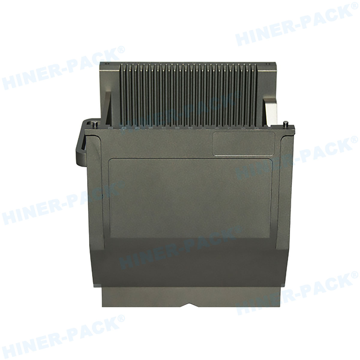
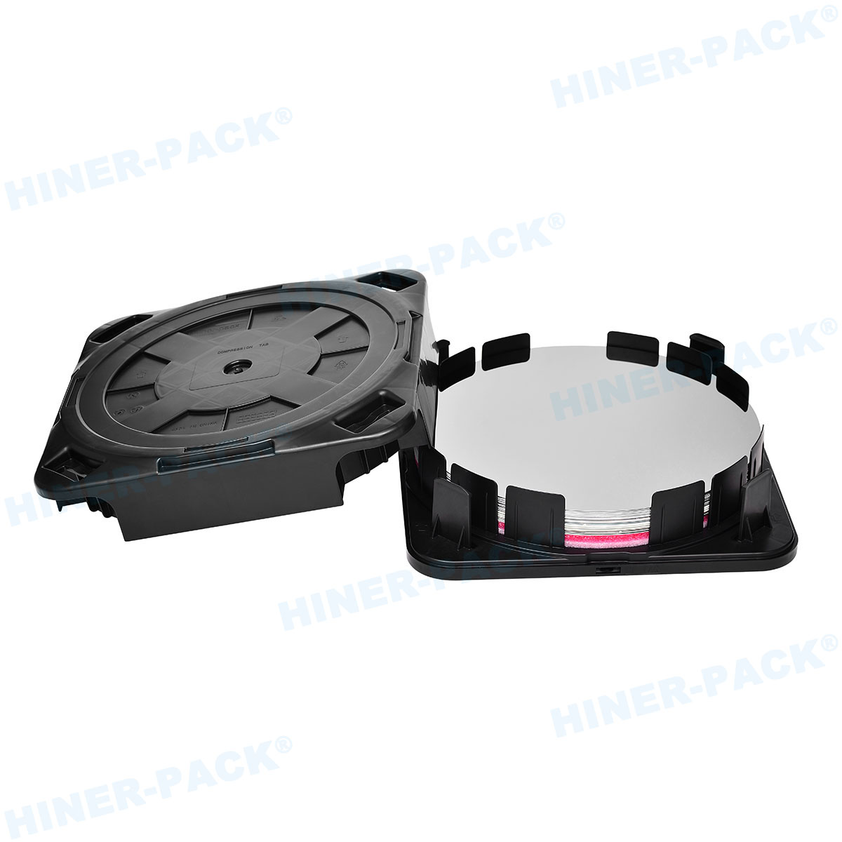
Mechanical Shock and Vibration: During air or road transport, packages are subjected to significant G-forces. A proper wafer box for safe transport features precisely engineered interior supports, cradling each wafer individually to prevent contact, chipping, or cracking.
Electrostatic Discharge (ESD): Silicon wafers are extremely sensitive to ESD, which can silently damage circuits without any visible signs. ESD-safe materials are non-negotiable in a wafer transport carrier to safely dissipate any static charges.
Moisture and Outgassing: Humidity can corrode delicate metallic layers. Furthermore, low-quality plastics can "outgas" chemical vapors that contaminate wafer surfaces. Materials used in high-quality boxes are certified for low outgassing and often include options for humidity control.
The cost of failure is immense. A compromised shipment can lead to scrapped wafers, production delays, and missed deadlines, erasing profit margins and damaging supplier relationships. This is why companies like Hiner-pack focus exclusively on engineering solutions that mitigate these risks entirely.
Beyond the Standard: Key Considerations When Choosing Your Wafer Shipping Box
Selecting a wafer box for safe transport is not a one-size-fits-all process. The right choice depends on several critical factors related to your specific wafers and logistics.
1. Material Science: The Foundation of Protection
The material of the box is its first line of defense.
PFA (Perfluoroalkoxy) and PTFE: These high-purity plastics are the gold standard for front-end processes. They offer excellent chemical resistance, extremely low particulate generation, and can withstand high temperatures for cleaning.
Conductive and Static-Dissipative Plastics (e.g., PP, PC with carbon fillers): Essential for protecting against ESD, these are commonly used for back-end processes and general transport. They channel static charges away from the wafers safely.
Metal Hybrids: Some designs incorporate metal shells for extreme durability, with non-Marring plastic interiors to protect the wafer surface.
2. Design and Mechanical Integrity
The internal design is what physically cradles the wafer.
Wafer Slot Pitch: The spacing between slots must be precise to prevent wafer-to-wafer contact, even under shock.
Robust Latching Mechanisms: A secure, reliable latch is crucial to prevent the box from accidentally opening during transit. A failed latch can mean a total loss.
Stackability and Compatibility: Boxes must be stackable to optimize shipping space and must be compatible with standard automated handling equipment (AMHS) at both the sending and receiving facilities.
3. Compliance and Certification: Your Assurance of Quality
Never assume a box is safe. Look for:
SEMI Standards: Compliance with SEMI standards (e.g., SEMI M1, M13, M31) is a baseline requirement. This ensures dimensional accuracy and material purity.
ESD Certification: Proof that the material meets the required surface resistance for safe static dissipation.
Cleanroom Class Certification: Documentation showing the box is manufactured and packaged in a certified cleanroom to prevent initial contamination.
Brands that prioritize these details, such as Hiner-pack, provide full traceability and certification with their products, giving engineers and supply chain managers peace of mind.
The Economics of Protection: Cost vs. Value in Wafer Transport
It's tempting to view a wafer box for safe transport as a commodity where the lowest price wins. This is a dangerous fallacy. The true cost must be calculated on a total-cost-of-ownership basis.
The Price of Failure: The cost of a single ruined 300mm advanced wafer can run into tens of thousands of dollars. A single failure can eclipse the savings from hundreds of cheaper boxes.
Reusability and Longevity: A high-quality wafer shipping box is designed for hundreds of cycles. While the initial investment is higher, the cost-per-trip becomes negligible compared to single-use or low-durability alternatives.
Operational Efficiency: Boxes that are easy to handle, clean, and integrate into automated systems reduce labor costs and prevent bottlenecks.
Investing in a robust wafer transport carrier from a reputable supplier is not an expense; it is a form of insurance for your most critical assets.
Innovations in Wafer Carrier Technology: Smarter, Safer Transport
The technology behind the wafer box for safe transport is continuously evolving. The latest innovations focus on adding intelligence and further reducing risk.
RFID and IoT Integration: Embedded RFID tags allow for seamless tracking of the box and its contents throughout the global supply chain. This provides real-time visibility and improves inventory management.
Advanced Sensor Carriers: Some carriers now include integrated sensors that monitor and record conditions during transit, including shock, temperature, and humidity. This data is invaluable for validating the safe transport process and identifying issues in the logistics chain.
Lightweight, High-Strength Composites: New material blends are being developed to reduce the weight of boxes (lowering shipping costs) while maintaining or even improving their structural integrity and protective qualities.
Forward-thinking manufacturers are at the forefront of these developments, ensuring that the humble wafer box continues to meet the escalating demands of the semiconductor industry.
In the intricate dance of semiconductor manufacturing, every component must perform flawlessly. The wafer box for safe transport is a foundational element in this process, a guardian of value and a facilitator of innovation. Choosing the right partner for your wafer packaging needs is a strategic decision that directly impacts your bottom line and operational resilience.
It is essential to work with specialized suppliers who understand the physics of protection, the chemistry of materials, and the realities of global logistics. Companies like Hiner-pack have built their reputation on providing engineered solutions that go beyond mere containment, offering the reliability and advanced features that modern semiconductor companies require. When the integrity of your wafers is on the line, the box you choose is the most important decision you'll make for their journey.
Frequently Asked Questions (FAQs)
Q1: What is the main difference between a front-end and a back-end wafer box for safe transport?
A1: Front-end wafer transport carriers are designed for the most sensitive, pristine wafers directly from the fab. They are typically made from ultra-pure materials like PFA, have extremely low particulate generation, and are used in the most critical manufacturing stages. Back-end boxes are used after the wafers have been diced into chips. They still require ESD protection and mechanical safety but may use different, cost-effective materials like static-dissipative polypropylene, as the absolute highest level of purity is slightly less critical.
Q2: How many times can a typical wafer shipping box be reused?
A2: A high-quality wafer box for safe transport from a reputable manufacturer is designed for hundreds of cycles—often 500 or more. The actual lifespan depends on the material, the handling conditions, and the rigor of the cleaning processes between uses. Regular inspection for wear, cracks, or latch failure is crucial to determine when a box should be retired.
Q3: Are there standardized sizes for wafer boxes?
A3: Yes, the industry follows SEMI standards which define the critical dimensions for wafer shipping boxes. Standards like SEMI M1 for 150mm wafers and E1.2 for 300mm wafers ensure interoperability between different manufacturers' boxes and the automated handling equipment used in fabs and assembly plants. This standardization is vital for a smooth global supply chain.
Q4: Besides the box itself, what else is needed for safe international wafer shipment?
A4: A robust wafer box for safe transport is the core, but it is part of a larger system. For international shipping, the box is placed inside a secondary packaging, usually a specially designed shipping container with additional cushioning (like foam or inflatable bags) to absorb external shock. This entire package is then placed inside a sealed, moisture-barrier bag, often with a humidity indicator card, before being packed in an outer corrugated box.
Q5: How do I properly clean and maintain a wafer transport carrier?
A5: Proper maintenance is key to longevity and performance. The process typically involves automated or manual cleaning with deionized (DI) water and high-purity, non-ionic detergents in a controlled cleanroom environment. After cleaning, the boxes are dried in particle-free dryers. It is critical to avoid harsh chemicals or abrasive tools that can damage the surface and generate particles. Always follow the manufacturer's specific cleaning and handling guidelines.


