
In the high-stakes world of semiconductor manufacturing, the safe transit of silicon wafers is not just a logistical step; it's a pivotal point where billions of dollars in potential revenue are on the line. A single particle of dust, a minor static discharge, or an imperceptible vibration during transport can render a wafer useless. At the heart of mitigating these risks lies a seemingly simple yet profoundly engineered component: the wafer box with lid for transport. This article delves into the five critical factors that every semiconductor professional must consider when choosing this essential carrier, ensuring integrity from the cleanroom to the fab.
Why Your Standard Wafer Carrier Isn't Enough for Shipping
Many facilities use standard front-opening unified pods (FOUPs) or open cassettes for in-fab handling. However, transporting wafers between facilities, even across a campus, demands a higher level of protection. A dedicated wafer box with lid for transport is designed specifically for this purpose. It creates a sealed, controlled microenvironment that shields wafers from:
Physical Shock and Vibration: Unlike stationary carriers, transport boxes are built with robust materials and often feature internal cushioning or compliant latches to absorb energy from handling and vehicular movement.
Particulate Contamination: The seal between the base and the lid is paramount. High-quality boxes achieve Class 1 or better cleanroom compatibility, preventing external contaminants from entering.
Moisture and Outgassing: Critical for advanced nodes, these boxes are made from low-outgassing polymers that won't release volatile chemicals, and the seal helps maintain a stable humidity level.
Electrostatic Discharge (ESD): Dissipative or conductive materials are used to prevent a buildup of static electricity, which can attract particles and damage delicate circuit features.
Factor 1: Material Composition and Purity
The very substance of the wafer shipping box is its first line of defense. Not all plastics are created equal.
PFA, PP, and PEEK: Perfluoroalkoxy (PFA) is the gold standard for high-purity applications due to its excellent chemical resistance and ultra-low particulate shedding. Polypropylene (PP) offers a cost-effective and very clean alternative for many processes. For extreme thermal or mechanical stress, Polyether Ether Ketone (PEEK) may be used.
Carbon Loaded and Static-Dissipative: To control ESD, materials are often compounded with carbon or other additives. It's crucial to specify the required surface resistance (e.g., 10^6 to 10^9 ohms/sq for dissipative) to match your wafer sensitivity.
Low-Metallic, Low-Ionic Contamination: The material must be certified to not introduce metallic or ionic contaminants that could poison the wafer surface during transit. This is a key area where suppliers like Hiner-pack provide detailed material certification data sheets.
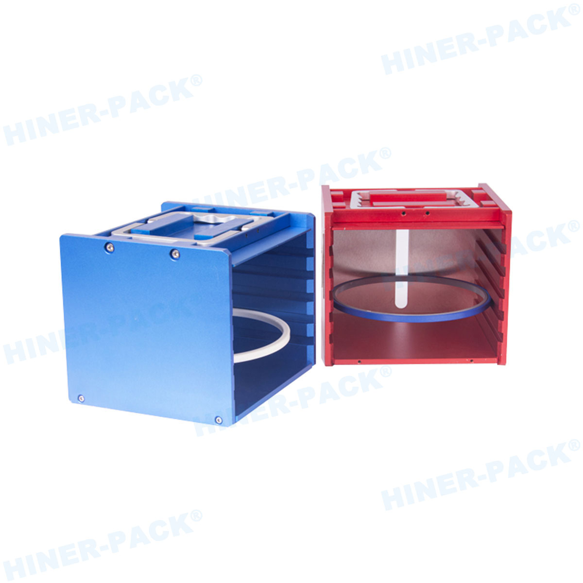
Factor 2: Mechanical Design and Latching Mechanism
A weak latch or a poorly designed hinge is a single point of failure with catastrophic potential. The mechanical integrity of a wafer transport container with lid is non-negotiable.
Latch Reliability: Look for positive-locking, tool-less latches that provide both an audible and tactile "click" to confirm secure closure. Redundant latching systems are a premium feature for the most critical shipments.
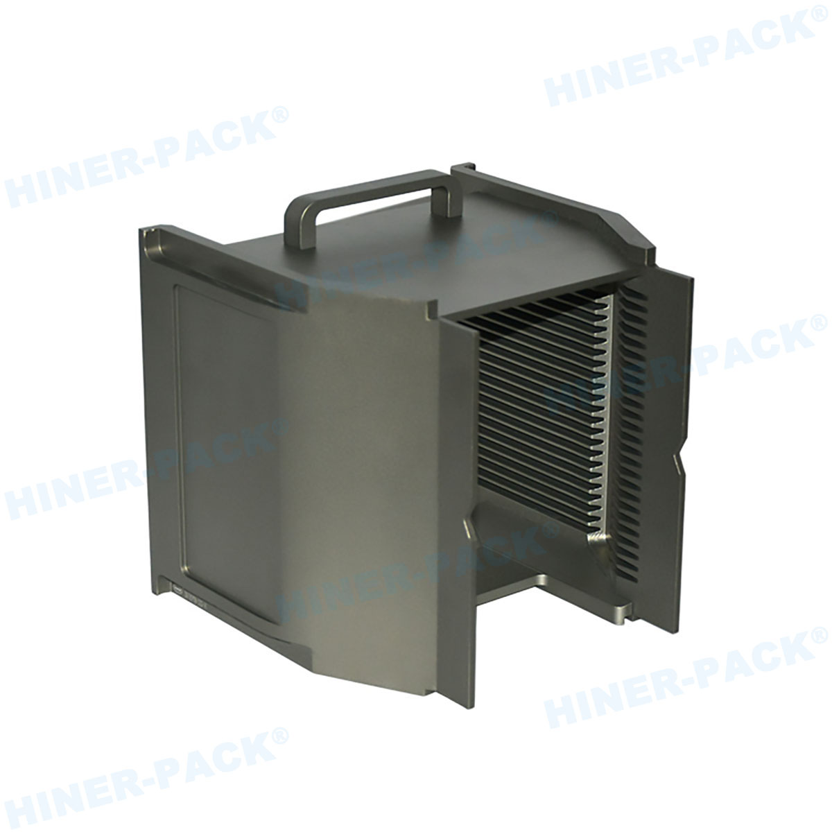
Stackability: Efficiency in logistics is key. A well-designed box will be stackable when full and when empty, saving precious space and ensuring stability during palletized transport.
Handle and Ergonomics: A properly designed handle allows for secure, single-handed carrying without compromising the operator's grip or risking a drop, especially when wearing cleanroom gloves.
Factor 3: Sealing Performance and Contamination Control
The seal is what transforms a box with a lid into a true protective wafer box with lid for transport.
Gasket Material: Common options include silicone, Teflon-coated silicone, or fluoropolymer gaskets. The choice depends on the required level of chemical inertness and compression force.
Seal Design: A double-channel seal often provides superior protection compared to a single lip, creating two barriers against particles and moisture.
Cleanroom Compatibility: The entire unit should be designed for easy cleaning and should be certified to meet or exceed the particulate standards of the environments it will be used in.
Factor 4: Capacity and Wafer Size Compatibility
One size does not fit all. The wafer shipping container must be precisely matched to the wafer diameter and quantity.
Standard Sizes: While 200mm and 300mm are the most common, the industry is rapidly adopting 450mm for future nodes. Ensure your supplier offers the size you need.
Capacity: Standard capacities are 25 wafers, but 13- or 6-wafer shippers are common for smaller, high-value lots. The internal slot pitch and depth must be exact to prevent wafer movement and contact.
Custom Configurations: For specialized applications like MEMS or photonic wafers, you may need a custom wafer transport box with lid. Suppliers with strong engineering capabilities, such as Hiner-pack, can develop tailored solutions for unique requirements.
Factor 5: Compliance, Traceability, and Total Cost of Ownership (TCO)
The final factor extends beyond the physical box to its lifecycle and integration into your quality system.
SEMI Standards: The box should be compliant with relevant SEMI standards (e.g., SEMI E1 for 300mm carriers), ensuring interoperability and reliability.
Traceability Features: Integration points for RFID tags or barcodes are essential for lot control and supply chain visibility.
TCO vs. Purchase Price: The cheapest box can be the most expensive. Calculate TCO by considering durability (number of trips before failure), cleanability (cost of consumables and labor), and its impact on yield. A robust wafer box with lid for transport from a quality-focused manufacturer pays for itself by preventing a single wafer loss.
Selecting the right wafer box with lid for transport is a technical decision with direct financial implications. It is an investment in yield protection and supply chain resilience. By rigorously evaluating the material, mechanical design, sealing, compatibility, and compliance, you can make an informed choice that safeguards your most valuable assets. As you evaluate your options, consider the engineered solutions offered by specialists like Hiner-pack, whose focus on precision and purity aligns with the uncompromising demands of the global semiconductor industry.
Frequently Asked Questions (FAQs)
Q1: What is the main difference between a standard wafer cassette and a dedicated wafer box with lid for transport?
A1: A standard wafer cassette is primarily designed for holding wafers within the controlled environment of a fab or process tool. A dedicated wafer box with lid for transport is engineered for the rigors of shipping. It features a sealed lid with a robust gasket to block contaminants and moisture, a heavy-duty latching mechanism to prevent accidental opening, and enhanced structural integrity to protect against physical shock and vibration during transit.
Q2: How many times can I typically reuse a wafer shipping box?
A2: The lifespan of a high-quality wafer transport container with lid can be hundreds of cycles if properly maintained. The key factors affecting longevity are the material's durability, the integrity of the latching mechanism over time, and, most importantly, the effectiveness of the cleaning and inspection processes between uses. Always inspect the box, particularly the gasket and latches, for signs of wear before each use.
Q3: Are there specific cleaning procedures for these transport boxes?
A3: Yes, strict cleaning protocols are essential. Typically, this involves using high-purity DI water and specialized, low-residue cleaning agents in a controlled environment, often with ultrasonic or spray tools. The procedure must be validated to ensure it does not damage the box or leave behind contaminants. The manufacturer, such as Hiner-pack, usually provides detailed cleaning and handling guidelines.
Q4: Can I get a custom-designed wafer box for non-standard wafer sizes or shapes?
A4: Absolutely. Many leading suppliers offer custom design services for a custom wafer transport box with lid. This is common for fragile MEMS wafers, compound semiconductors like GaAs, or other non-standard geometries. These custom solutions can include tailored slot designs, specific material choices, and unique latching mechanisms to meet exact application requirements.
Q5: Why is ESD protection so critical in a wafer shipping container?
A5: Electrostatic discharge (ESD) or even static attraction can be devastating. A static charge can directly damage nanoscale features on a wafer. More commonly, it turns the box and wafers into a magnet for airborne particulate contamination, which causes defects and kills yield. A proper wafer box with lid for transport uses static-dissipative materials to safely bleed away any charge, protecting the wafers throughout the logistics chain.


