
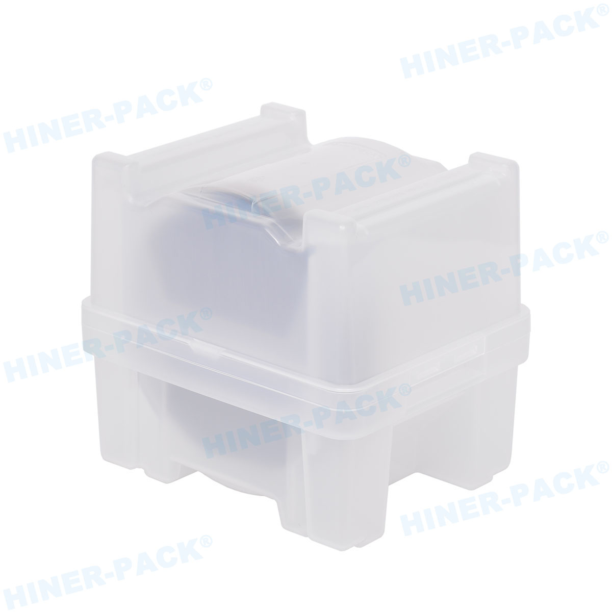
In advanced semiconductor packaging—fan-out wafer-level packaging (FOWLP), 3D-IC, hybrid bonding, and wafer thinning—the component often overlooked but constantly under extreme stress is the wafer carrier. When a wafer carrier for sale enters your procurement pipeline, it is not merely a shipping box; it is a process-critical tool that influences particle contamination, die shift, edge chipping, and electrostatic discharge (ESD). For engineers and procurement managers, the challenge is not finding a supplier—it is identifying a carrier that matches thermal budgets, chemical resistance, and dimensional stability across backgrinding, temporary bonding, debonding, and dicing. This guide provides a technical framework based on polymer science, cleanroom protocols, and real-world failure modes.
Hiner-pack specializes in engineered wafer handling solutions, offering carriers that meet SEMI standards and custom specifications. Whether your process runs at 260°C for polyimide curing or requires low-outgassing materials for EUV lithography, understanding carrier attributes directly impacts yield. Below we dissect material selection, surface roughness, particle generation mechanisms, and purchase checkpoints.
1. Why Standard Wafer Carriers Fail in High-Stakes Packaging Processes
Many semiconductor fabs and OSATs (outsourced semiconductor assembly and test) still rely on generic carriers intended for storage or basic transport. However, advanced packaging introduces aggressive chemistries, elevated temperatures, and mechanical loads that degrade conventional carriers. Four failure modes dominate:
Thermal creep and warpage: Carriers subjected to repeated 150–250°C cycles (e.g., temporary bonding adhesive curing) develop permanent warpage, causing non-uniform vacuum chuck contact during debonding.
Particle shedding from uncoated surfaces: Standard machined carriers have micro-burrs and rough sidewalls that generate ≥0.3μm particles, leading to killer defects in fine-pitch copper pillars.
ESD-induced gate oxide damage: Carriers without controlled surface resistivity (≤1E6 Ω/sq) accumulate charge during dry environments (N2 purge or low humidity cleanrooms), damaging thin gate oxides in wafers with sensitive devices.
Chemical incompatibility with solvents: NMP, PGMEA, or diluted HF residues from cleaning processes cause surface crazing or extractable release, cross-contaminating subsequent processing baths.
Therefore, evaluating a wafer carrier for sale demands not just a price check but a full characterization of polymer grade, injection molding vs. machined finish, and certification data for particles, outgassing, and ionic contamination.
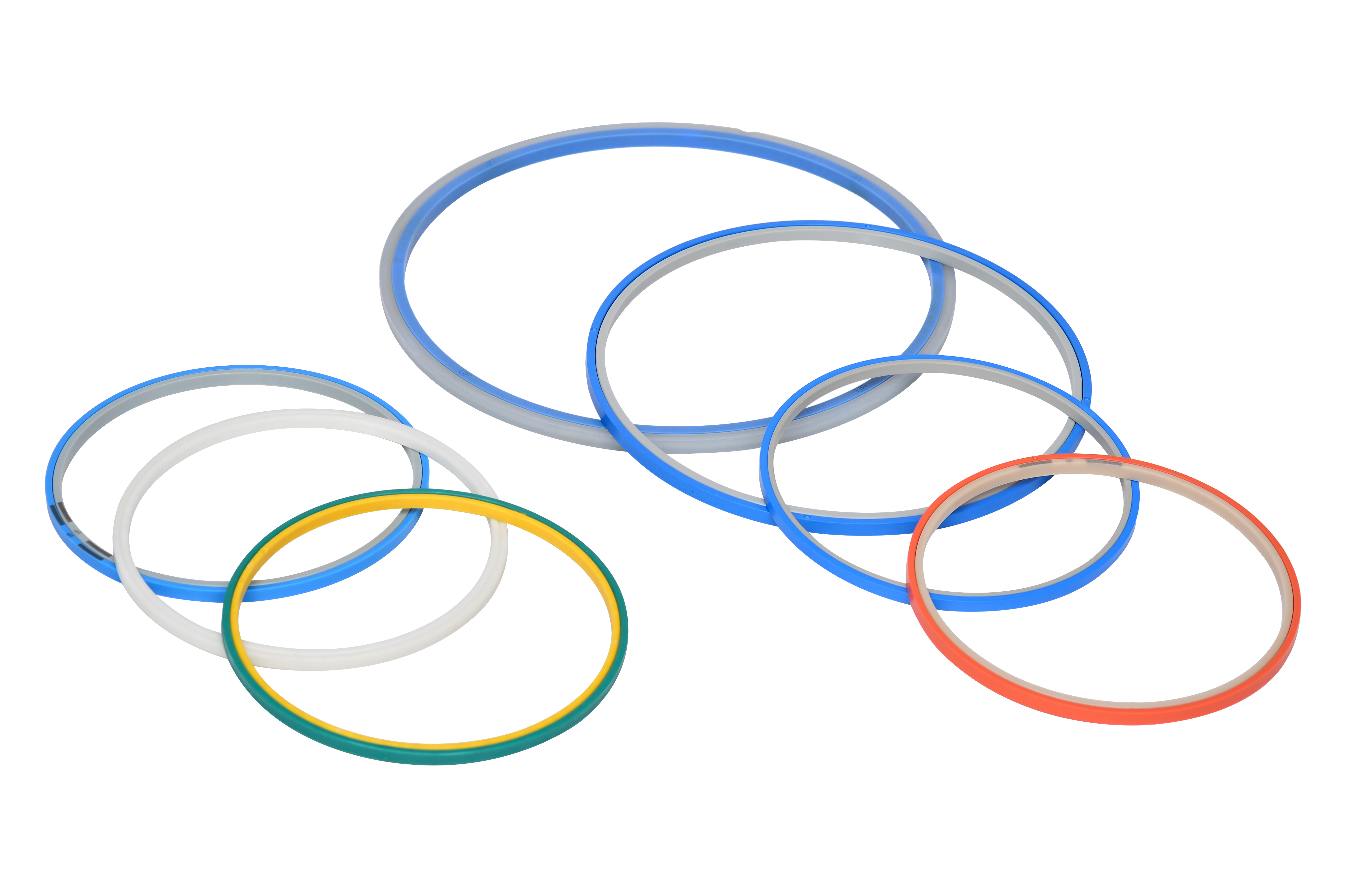
2. Material Science Deep Dive: PEEK, PFA, Anti-static PP and Their Application Windows
The semiconductor industry selects carrier substrates based on operating temperature, chemical exposure, and mechanical rigidity. Three material families dominate current packaging lines, each with trade-offs.
2.1 Polyetheretherketone (PEEK) – High-temperature stability
PEEK carriers withstand continuous use up to 260°C and peaks of 300°C, making them suitable for polyimide cure (PIQ) or wafer-level underfill reflow. PEEK exhibits low outgassing (NASA low outgassing certified grades available) and excellent hydrolytic stability. However, it is costly, and static dissipation requires carbon or carbon-nanotube filler which slightly reduces purity. For backgrinding processes with hot mounting tapes, PEEK maintains flatness within ±25μm across 300mm wafers.
2.2 Perfluoroalkoxy (PFA) – Extreme chemical resistance
PFA carriers are specified for wet etching, plating, and cleaning where aggressive acids (H2SO4, HF, HCl) or bases (TMAH) are present. Unlike PEEK, PFA does not absorb solvents, eliminating extractable metal ions that cause mobile ion contamination. The trade-off: lower mechanical modulus, requiring thicker carrier designs. For 200mm wafer handling in wet benches, PFA carriers offer service life beyond 5 years under constant chemical spray.
2.3 Anti-static Polypropylene (PP) – Cost-effective for ambient transport
Carbon-filled PP (surface resistivity 10^3 – 10^6 Ω/sq) provides ESD protection at a lower price point. Maximum continuous temperature is 85°C, limiting use to back-end assembly (die attach, wire bonding) or inter-fab transport. Many suppliers offer injection-molded PP carriers with integrated rib structures to prevent wafer warpage. When sourcing a wafer carrier for sale for ambient applications, PP provides an acceptable balance of particle control and cost.
Hiner-pack provides material selection guidance backed by TGA (thermogravimetric analysis) and FTIR (Fourier-transform infrared spectroscopy) reports, ensuring the carrier chemistry matches your exact fab process.
3. Performance Metrics That Define a Qualified Wafer Carrier
Industry standards (SEMI E15, E16, E42) specify dimensional and cleanliness criteria, but packaging engineers should request additional data from suppliers. Below are key performance indicators (KPIs) to verify before purchase.
Surface roughness (Ra) on wafer contact areas: ≤0.4μm Ra for 300mm carrier pockets to reduce particle generation. Higher roughness leads to micro-abrasion of wafer edge, creating silicon dust that migrates into optics or dispense nozzles.
Outgassing (by GC-MS): For vacuum processes like sputtering or ALD, outgassing rates must be <10 μg/cm² after 10 minutes at 125°C. Amides, slip agents, and unreacted monomers are common contaminants that redeposit onto chamber optics.
Ionic cleanliness (ROHIS-compliant extraction): Anion and cation levels (chloride, fluoride, sodium, ammonium) shall be below 0.2 μg/cm² to prevent corrosion of aluminum bond pads or copper re-distribution layers (RDL).
ESD decay time: From ±1000V to ±50V in <2 seconds at 15% RH, according to ANSI/ESD STM11.11. Slow decay risks charge accumulation during wafer transfer, especially when carriers slide on guide rails.
Flatness and stackability: After 100 cycles between 25°C and 125°C, warpage should not exceed 0.1mm per 100mm of carrier length. Stackability testing ensures automated storage/retrieval systems (ASRS) do not jam.
Reputable suppliers provide these metrics in a Certificate of Analysis (CoA). When evaluating a wafer carrier for sale, insist on batch-specific test data rather than generic brochures.
4. Application-Specific Carrier Selection: Thinning, Bonding, and Dicing
Different packaging steps impose conflicting requirements. A carrier suitable for wafer transport may fail during plasma dicing or temporary bonding. Below we map carrier features to process stations.
4.1 Backgrinding and Tape Mounting
During backgrinding, carriers hold wafers via vacuum holes or mechanical clamping. Carriers must have recessed pockets to accommodate tape flags and edge trim residue. Anti-static PP or PEEK carriers with laser-marked wafer orientation flat slots are recommended. High flatness (±25μm) prevents wafer breakage when grinder chuck pressure exceeds 30kgf.
4.2 Temporary Bonding / Debonding (TBDB)
For ultra-thin wafer handling (≤50μm), a rigid carrier (often glass or silicon) supports the wafer through spin-coating, bonding, and laser debonding. However, polymer carriers are used as shipping and storage carriers before and after TBDB. They must tolerate residual adhesive solvents (e.g., cyclopentanone, anisole) without swelling. PFA carriers show excellent solvent resistance, whereas PEEK exhibits slight swelling in polar aprotic solvents, causing dimension changes. Confirm chemical compatibility via 24-hour immersion test at 60°C.
4.3 Dielectric Curing and Reflow
Carriers entering convection ovens or hot plates for polyimide, PBO, or BCB curing must survive 250–350°C (short peaks). Only specific polyimide-rated PEEK carriers or carbon-reinforced PEEK are suitable. Standard PP carriers will permanently deform. Look for carriers with “elevated temperature stable” marking and thermal conductivity data to ensure even wafer heating.
4.4 Plasma Dicing and Dry Etch
Plasma dicing chambers operate at low pressure with fluorine-based gases (SF6, CF4). Carriers exposed to plasma environment must avoid halogen outgassing, which corrodes chamber walls. PFA and specially sealed PEEK carriers are preferred. Additionally, carriers must be electrically grounded to avoid arcing damage to the dicing mask.
Hiner-pack offers a customizable series with ESD-safe coatings and thermal rating reports, directly addressing TBDB and plasma dicing requirements.
5. Procurement Checklist: What to Verify Before Ordering a Wafer Carrier
Purchasing managers and process engineers should form a cross-functional checklist. Missing one parameter leads to line stoppages or yield excursions. Below is a recommended validation flow.
Step 1 – Cleanroom certification: Carrier must be double-bagged in Class 100 (ISO 5) environment with particle count ≤200 particles >0.1μm per carrier (verified by liquid particle counter).
Step 2 – Compatibility matrix: Request the supplier’s chemical compatibility table with 30+ solvents and acids used in your fab (NMP, developer, BOE, etc.).
Step 3 – Dimensional report: For 300mm carriers, pocket diameter, slot pitch, and overall dimensions must comply with SEMI E47. Reject any supplier that does not provide CMM (coordinate measuring machine) data.
Step 4 – Lot traceability: Each carrier should be laser-marked with batch number and date of manufacture. This enables root-cause analysis if contamination emerges downstream.
Step 5 – Sample testing in your process: Order 5–10 sample carriers and run a full production shift. Measure particle adders before and after wafer transfer using a surface scanner (e.g., KLA Surfscan).
A wafer carrier for sale should include a service agreement for requalification after cleaning cycles. Some suppliers like Hiner-pack provide periodic recertification to extend carrier life and maintain compliance.
6. Future Trends: Embedded RFID and Smart Carriers for IIoT Integration
Semiconductor fabs are adopting industry 4.0 practices, where wafer carriers become data nodes. Passive UHF RFID tags embedded in carrier rims store process history: number of cleaning cycles, peak temperatures encountered, and ESD events. This data integrates with MES (manufacturing execution system) to predict carrier replacement. Advanced carriers also feature temperature loggers for oven tracking. When evaluating suppliers, ask about RFID integration without increasing particle shedding. Hiner-pack currently offers RFID-ready designs with custom encapsulation to avoid contamination.
Additionally, lighter-weight carriers through structural simulation (topology optimization) reduce robotic arm payload and energy consumption. However, stiffness cannot be compromised. Expect to see more glass-fiber reinforced PEEK composite carriers that achieve 20% weight reduction.
Frequently Asked Questions (FAQ) on Wafer Carrier Sourcing
Q1: What is the difference between a wafer shipping carrier and a process carrier?
A1: Shipping carriers (often FOUP-like or single-wafer containers) prioritize mechanical protection and shock absorption during transport, typically made from low-cost anti-static PP. Process carriers, on the other hand, are designed for in-line equipment (grinders, coaters, etc.) and require high dimensional accuracy, chemical resistance, and low outgassing. Process carriers are frequently cleaned and reused, while shipping carriers may be single-use. When looking for a wafer carrier for sale, verify whether it meets SEMI process carrier standards (E142 for FOSB) or only shipping specifications.
Q2: Can I use the same wafer carrier for wet etching and high-temperature curing?
A2: No, a single material rarely satisfies both aggressive wet chemistry and high-temperature exposure. PFA handles wet etching perfectly but its maximum continuous use temperature is around 260°C, and it softens above 280°C. PEEK can survive 300°C but absorbs certain etchants (e.g., concentrated HF at elevated temperature). The best practice is dedicated carriers per process module or use PFA for wet sections and PEEK for thermal sections. Hiner-pack provides application-specific design reviews to avoid cross-use failures.
Q3: How often should wafer carriers be replaced?
A3: Replacement frequency depends on process severity. For carriers used only in ambient storage and transport, 3–5 years is typical if cleaned regularly. For carriers exposed to plasma, aggressive chemicals, or temperatures above 200°C, inspect every 12 months for warpage, surface pitting, or increased particle counts. Many fabs replace high-temperature PEEK carriers every 18–24 months. Always track carrier cycles in your MES. When purchasing a wafer carrier for sale, request expected lifetime data based on similar applications.
Q4: What cleaning procedures are safe for anti-static wafer carriers?
A4: Anti-static carriers (carbon-filled PP or PEEK) are sensitive to harsh oxidizers and strong acids that degrade the conductive filler. Acceptable cleaning methods: deionized water rinse, isopropyl alcohol (IPA) with ultrasonic agitation (max 5 min), or neutral detergent. Avoid acetone, NMP, or >5% nitric acid, as these leach carbon particles, increasing surface resistivity beyond safe limits. After cleaning, measure ESD decay time again. Hiner-pack provides validated cleaning protocols for their carrier lines.
Q5: Can I get carriers with custom pocket geometries for warped or thin wafers?
A5: Yes, many suppliers, including Hiner-pack, offer custom-machined or injection-molded carriers with adjustable pocket depth, edge support rings, or variable slot pitches for warped wafers (bow up to 2mm). For ultrathin wafers (<100μm), carriers may require full-area support mesh or porous vacuum chucks. When evaluating a custom wafer carrier for sale, provide your wafer bow distribution and thickness variation; the supplier then calculates optimal contact points to avoid stress fractures.
Ready to Specify Your Next Wafer Carrier? Request a Technical Consultation
Selecting a wafer carrier is a materials engineering decision that directly impacts packaging yield. Whether you need high-temperature PEEK for polyimide cure, chemically inert PFA for wet benches, or ESD-safe PP for assembly transport, the right carrier must come with verified cleanliness, thermal stability, and dimensional reports.
Hiner-pack engineers work with your process data to supply wafer carriers for sale that meet SEMI standards and custom parameters. We provide sample qualification kits, particle test data, and long-term reliability simulations.
For immediate technical support or a quotation, send your wafer size, process temperature range, and chemical exposure list to our engineering team. We respond within 24 business hours.
All inquiries receive a preliminary material recommendation and a checklist for carrier validation.


