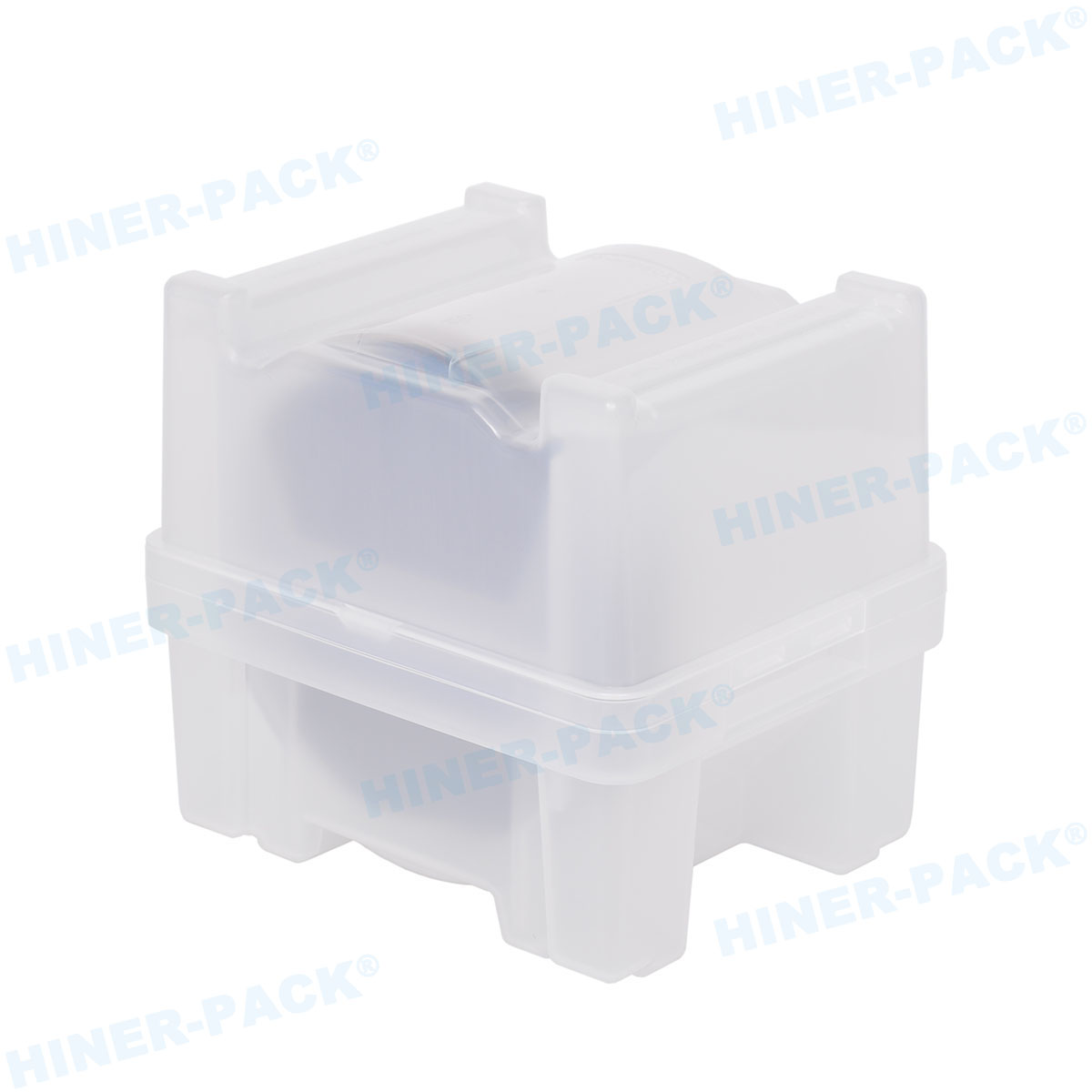
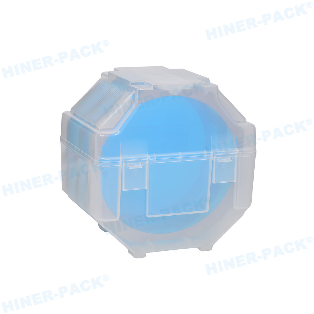
A wafer carrier
factory is not merely a molding shop—it is a specialized manufacturing
environment that combines material science, sub-micron metrology, and
contamination control protocols. The carriers produced in such facilities
directly affect wafer breakage rates, particle-induced defects, and
electrostatic discharge (ESD) failures in semiconductor fabs. This article
provides a detailed examination of what separates a commodity tray supplier from
a high-performance wafer carrier
factory that serves leading foundries and OSATs (outsourced semiconductor
assembly and test).
With over two decades of hands-on experience in wafer handling solutions, I
will break down the engineering steps, quality checkpoints, and
application-driven design rules that define a reliable manufacturing partner.
Hiner-pack operates one such
advanced facility, integrating in-house tooling, class 1000 cleanroom molding,
and full traceability systems.
1. Core Infrastructure of a Modern Wafer Carrier Factory: Cleanroom Classes
and Injection Molding Precision
The production environment for wafer carriers must match the cleanliness
levels of the fabs they serve. A professional wafer carrier
factory maintains at least ISO 7 (Class 10,000) cleanrooms for molding, with
assembly and packaging areas upgraded to ISO 5 (Class 100) or better. This
prevents airborne particles from embedding into carrier surfaces during
manufacturing. Beyond cleanrooms, key equipment includes:
Electric injection molding machines with closed-loop
process control, ensuring shot-to-shot consistency for cavities holding 200mm,
300mm, or panel-level substrates.
CNC machining centers for rapid tool modifications and
prototype carriers, enabling iterative design for warped wafers or non-standard
thicknesses.
Coordinate measuring machines (CMM) and optical profilers
to verify pocket depth (±15 µm), slot pitch, and coplanarity across the entire
carrier array.
Surface resistivity testers and ion chromatography for
validating ESD performance and extractable ion levels (often below 5 ppb for
sensitive nodes).
Each production lot undergoes statistical process control (SPC) on critical
dimensions. For carriers used in wet benches or high-temperature curing, the
factory must also provide post-molding annealing to relieve internal stresses,
preventing warpage when exposed to 200°C+ cycles.
2. Material Science and Customization Capabilities: Tailoring Carriers for
Specific Process Steps
Semiconductor processes require carriers resistant to chemicals, thermal
shocks, and static buildup. A competent wafer carrier
factory maintains a library of engineered thermoplastics and offers
application-specific recommendations. Common base polymers and their process
windows include:
PEEK (polyether ether ketone): Continuous use to 260°C,
excellent for burn-in, curing, and high-temperature handling. Minimal outgassing
and compatible with aggressive solvents like NMP and PGMEA.
PEI (polyetherimide): Good dielectric properties and creep
resistance; often specified for ESD-critical environments when loaded with
conductive fillers.
Conductive polycarbonate (PC): Cost-effective for shipping
and storage carriers, surface resistivity 10⁵–10⁹ Ω/sq to avoid
tribocharging.
PFA/PTFE: For wet etching and plating lines where
concentrated HF, H₂SO₄, or KOH are used; these fluoropolymers provide near-inert
behavior.
Beyond material selection, the factory’s engineering team must adapt cavity
profiles. For thin wafers (under 100 µm), edge-grip designs or vacuum-assisted
pockets replace traditional support ribs. For warped wafers (bow >2mm), the
factory can generate 3D scans of sample wafers and produce form-fitting slot
surfaces. Hiner-pack offers such custom
tooling with lead times as short as 4 weeks for prototype iterations.
3. Quality Assurance Protocols: From Raw Material Receiving to Outgoing
Shipment
High-volume wafer fabs cannot tolerate batch-to-batch variation. Therefore, a
reliable wafer carrier
factory implements a multilayered QA system. The following checkpoints are
industry standard:
Incoming material verification: Each resin lot is tested
for melt flow index, ash content, and metal impurity levels (ICP-MS for 15+
elements).
In-process monitoring: Cavity pressure sensors and mold
temperature mapping ensure filling uniformity. Automated vision systems inspect
each molded part for flash, sinks, or short shots.
Dimensional audit: Sample carriers from every cavity (in
multi-cavity tools) are measured on a CMM. Critical dimensions include slot
width, wafer support height, and edge clearance.
Particle and cleanliness test: Carriers are rinsed with DI
water, then analyzed for particle shedding per SEMI E49.6 (≤0.1 particles/cm²
for particles >0.3 µm is typical for high-end products).
ESD verification: Surface and volume resistivity measured
per ANSI/ESD STM11.11 or ASTM D257. Carriers are also checked for electrostatic
decay time.
Documentation packages accompany each shipment, including certificate of
conformance, dimensional reports, and cleanliness test data. This traceability
allows fabs to correlate carrier batches with yield performance—an essential
feature for automotive or medical device semiconductor lines.
4. Solving Field Failures: How a Wafer Carrier Factory Addresses Common Fab
Complaints
Even well-designed carriers encounter issues in production environments. A
proactive factory uses root cause analysis to modify designs or processes. Below
are frequent problems and engineering responses:
Cross-slot wafer scratching: Caused by insufficient pitch
or sharp slot edges. The factory solution involves increasing slot pitch by
0.2–0.5mm, radiusing all contact edges, and applying a lubricious coating (MoS₂
or PTFE) on ribs.
Carrier sticking to wafer after high-temperature step: Often due to thermal expansion mismatch or surface adhesion. The factory can add
micro-structuring (dimples) to reduce contact area and select polymers with
lower coefficient of friction at elevated temperatures (e.g., carbon-filled
PEEK).
Electrostatic damage during automated handling: Standard
carriers may not provide adequate grounding paths. Factories respond by
integrating conductive inserts, designing grounding pin features, or switching
to inherently dissipative polymer alloys (volume resistivity 10⁶–10⁹ Ω·cm).
Carrier warpage after repeated cleaning cycles: Residual
molding stresses or improper annealing cause deformation. The factory modifies
the molding parameters, adds a post-molding stress-relief step, or changes to a
more amorphous resin with lower shrinkage anisotropy.
Leading Hiner-pack provides an 8D report
for any quality deviation, along with corrective action samples within 10
working days—a level of service expected by top-tier semiconductor
manufacturers.
5. New Process Requirements: Fan-Out Packaging, Panel-Level Handling, and
High-Temperature Carriers
As the industry transitions from conventional wafer-level packaging to
panel-level packaging (PLP) and hybrid bonding, wafer carrier
factory capabilities must evolve. For fan-out wafer-level packaging (FOWLP),
reconstituted wafers have varying thicknesses and edge profiles. Carriers now
need adjustable side supports or compliant materials to accommodate non-uniform
wafers.
In panel-level processing (510mm x 515mm or larger), traditional round wafer
carriers are replaced by rectangular panel carriers, but the same design
principles apply: low particle generation, ESD control, and thermal stability up
to 300°C for dielectric curing. A forward-thinking factory invests in
large-platen injection molding machines (clamping force > 800 tons) and CNC
routers capable of handling panel-sized substrates.
Additionally, temporary bonding and debonding carriers (glass or silicon
carrier wafers) are increasingly used for thin-wafer handling. While these are
not plastic, some factories produce protective polymer rings and edge-grip
fixtures that interface with glass carriers. The key is collaboration—the
factory must be willing to co-develop solutions with the fab’s process
integration team.
Frequently Asked Questions (FAQs) – Wafer Carrier Factory &
Manufacturing Standards
Q1: What certifications should I look for when selecting a wafer
carrier factory?
A1: Essential certifications
include ISO 9001:2015 (quality management) and ISO 14001 (environmental). For
cleanroom manufacturing, look for ISO 14644-1 classification (Class 7 or
better). SEMI S2/S8 compliance for equipment safety and ESD Association
certification (ANSI/ESD S20.20) are also strong indicators. A reputable wafer carrier
factory will gladly share these certificates.
Q2: How does a wafer carrier factory validate particle performance
for carriers used in sub-10nm fabs?
A2: Factories
use liquid particle counters (LPC) and optical surface scanners to quantify
shedding. The standard test involves dynamic agitation (vibration or rotation)
followed by particle extraction and measurement per SEMI E49.6. For sub-10nm
nodes, the limit is often <0.05 particles/cm² ≥0.1 µm. The factory should
also provide outgassing analysis (via GC-MS) to ensure no volatile
condensables.
Q3: Can a wafer carrier factory produce carriers for non-standard
wafer sizes (e.g., 150mm, 200mm or custom
substrates)?
A3: Yes, most factories can supply
carriers for diameters from 100mm to 300mm, as well as small quantities for
R&D. Custom rectangular carriers for SiC or GaN substrates are also
possible. The key is providing detailed drawings or sample substrates. Many
factories, including Hiner-pack, offer low-volume
prototyping via CNC machining before committing to injection molding
tooling.
Q4: How many cycles can a typical process carrier withstand before
requiring replacement?
A4: Cycle life depends on
process severity. For aggressive wet etching at 80°C, carriers may last 300-500
cycles before showing wear or increased particle shedding. For less demanding
storage and handling, thousands of cycles are possible. A reliable factory will
provide accelerated life test data for each material-grade combination and
recommend requalification intervals.
Q5: What is the typical lead time for custom injection molding
tooling for wafer carriers?
A5: For a single-cavity
prototype tool (aluminum or soft steel), lead time ranges from 4 to 6 weeks. For
production-grade multi-cavity hard steel tools (up to 4 cavities for 300mm
carriers), 8 to 12 weeks is typical. The timeline includes mold flow analysis,
tool design, sampling, and dimensional validation. Expedited services are
available for urgent projects.
Need a reliable partner for
high-precision wafer carriers? The engineering team at Hiner-pack is ready to review
your wafer specifications, process conditions, and required cleanliness levels.
We offer free preliminary design reviews and sample runs for evaluation.
Send your wafer carrier inquiry now – include wafer
diameter, thickness range, process temperature, chemicals involved, and ESD
requirement. We will respond with a customized proposal, dimensional drawings,
and material recommendations within 24 hours. Click here to submit
your factory-direct inquiry →


