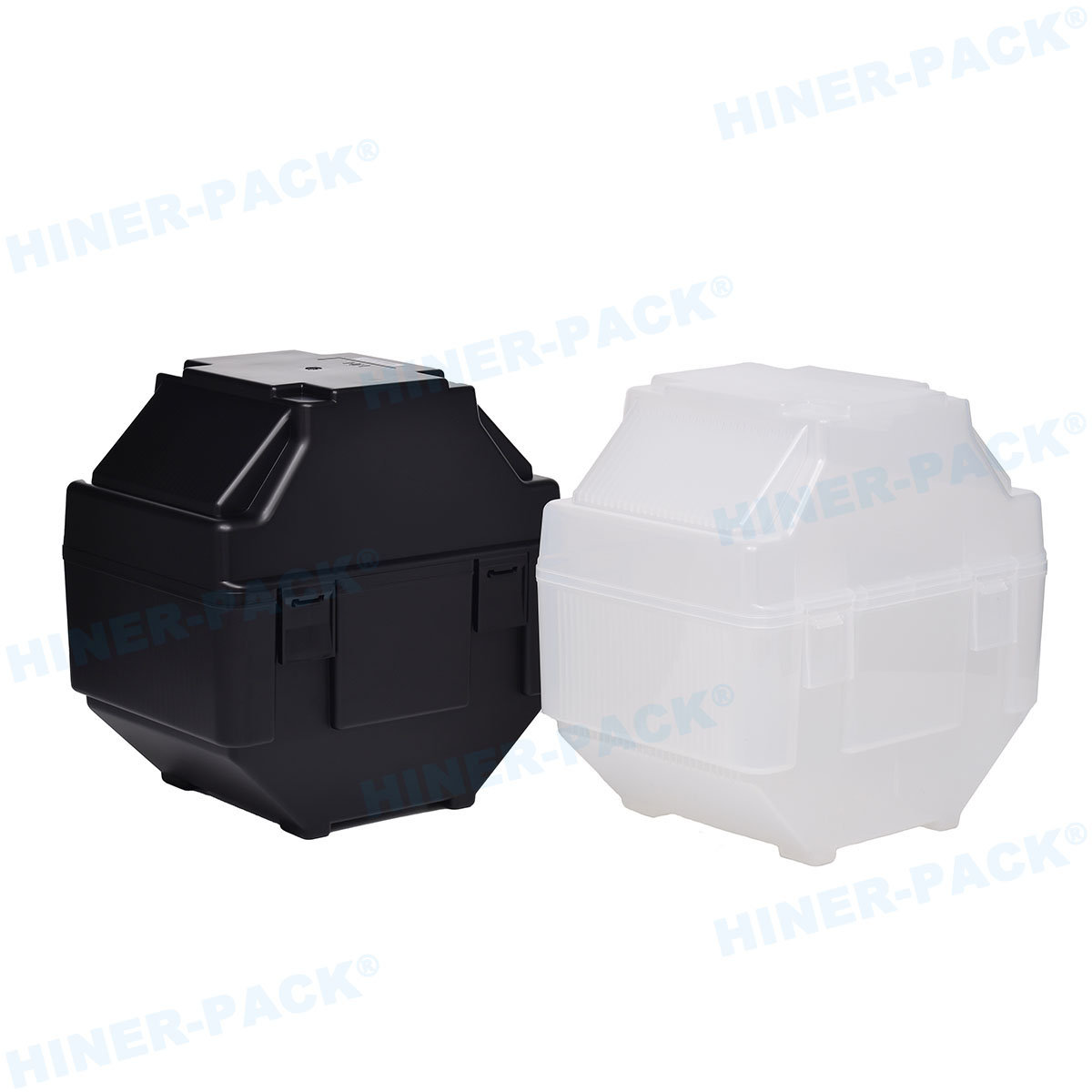
Wafer Carrier Performance Metrics: 7 Critical Factors for Sub-5nm Semiconductor ManufacturingThe relentless pursuit of geometric scaling—from 7nm to 3nm and beyond—has placed unprecedented demands on every component within the wafer fab ecosystem. Among these, the wafer carrier is no longer a passive shipping or storage box. In modern 300mm fabs leveraging automated material handling systems (AMHS), it functions as a micro-environment, a precision alignment interface, and a primary defense against yield-killing contaminants. As a B2B content strategist specializing in semiconductor materials, I’ve observed that the industry’s shift to angstrom-scale nodes necessitates a fundamental rethink of carrier materials, surface engineering, and electrostatic discharge (ESD) management. This analysis dissects the engineering rigor behind next-generation carriers, incorporating data-driven insights from leading suppliers such as Hiner-pack, and maps out actionable strategies for fab managers and procurement teams.
1. The Evolving Role of the Wafer Carrier in Advanced Fabs
Historically, a wafer carrier was perceived merely as a cassette for transport between process tools. Today, with the proliferation of 300mm Front Opening Unified Pods (FOUPs) and Front Opening Shipping Boxes (FOSBs), the carrier has become a critical process interface. Its functions now include:
Contamination Control: Maintaining ISO Class 1 or better cleanliness internally, with particle shedding limits below 0.1 particles/cm² at ≥0.1 μm.
Moisture & Gas Management: Minimizing outgassing (total organic carbon < 0.01 μg/cm²) to prevent defect formation in photolithography and etching stages.
ESD Protection: Surface resistivity in the range of 10³ to 10⁵ Ω/sq to dissipate charge without damaging delicate gate oxides.
Mechanical Precision: Maintaining slot-to-slot pitch uniformity within ±0.1 mm to accommodate increasingly thin wafers (down to 775 μm for 300mm) and fragile backside films.
These demands are codified in SEMI standards E1.9, E15.1, and E47, which define everything from kinematic coupling dimensions to purge efficiency. Non-compliance or even minor deviations in carrier geometry can lead to tool jams, wafer breakage, or cross-contamination—events that can cost a fab upwards of $50,000 per hour in downtime.
2. Material Science Breakthroughs: Beyond PFA and PP
The dominant materials for wafer carriers have long been polypropylene (PP) and perfluoroalkoxy (PFA) due to their chemical inertness. However, advanced nodes (5nm and below) require carriers that offer superior dimensional stability at elevated temperatures (up to 130°C in certain degassing processes) and lower ionic contamination. Emerging material solutions include:
2.1 Carbon-Fiber Reinforced PEEK (Polyether Ether Ketone)
PEEK composites offer higher stiffness, lower coefficient of thermal expansion (CTE ~20 ppm/°C compared to PP’s 80–100 ppm/°C), and exceptional resistance to aggressive chemicals like hydrofluoric acid vapor. While costlier, these carriers reduce particle generation from mechanical friction and maintain precise alignment during automated handling.
2.2 Static-Dissipative Coatings & Bulk-Doped Polymers
Traditional surface coatings can peel over time, creating contamination risks. Next-generation carriers from suppliers like Hiner-pack utilize bulk-doped polymers where conductive carbon nanotubes or inherently dissipative polymers (IDPs) are integrated throughout the resin. This ensures permanent ESD protection without the risk of coating delamination. Such designs achieve static decay times < 2 seconds per SEMI E129, crucial for protecting logic devices with gate lengths below 5nm.
3. Technical Deep Dive: Contamination Pathways and Mitigation
Contamination originating from the wafer carrier remains one of the top three yield detractors in leading-edge fabs. The contamination mechanisms are multi-faceted:
Abrasion-Induced Particles: Generated at kinematic coupling points and wafer contact edges. Advanced carriers employ soft-touch, low-contact area designs that minimize friction points by up to 40% compared to conventional cassettes.
Airborne Molecular Contamination (AMC): Outgassing from carrier plastics (e.g., amides, plasticizers) can deposit on wafer surfaces, leading to haze defects or gate oxide thinning. High-purity carriers undergo post-molding supercritical CO₂ cleaning and vacuum bake-out to reduce total outgassing below 0.5 μg/cm².
Metallic Contamination: Trace metals (Fe, Ni, Cu) from mold release agents or filler materials can migrate onto wafers. Top-tier carriers now adhere to SEMI S2/S8 standards with surface metal contamination < 0.01 ng/cm² for critical elements.
To address these, leading suppliers implement closed-loop manufacturing processes, including cleanroom molding (ISO 5 environment) and 100% automated optical inspection (AOI) for internal surface defects. Hiner-pack integrates in-line plasma treatment to modify surface energy, reducing particle adhesion by 30–50% according to internal test data from 300mm pilot lines.
4. AMHS Compatibility and Industry 4.0 Integration
Modern fabs are heavily automated, with Overhead Hoist Transports (OHTs) and stockers moving carriers continuously. A wafer carrier must not only be mechanically robust but also equipped with intelligent features. Key requirements now include:
RFID Tag Integration: Enables real-time tracking, lot genealogy, and predictive maintenance. Advanced carriers incorporate high-temperature RFID that withstands 130°C bake processes.
Standardized Kinematic Couplers: Conforming to SEMI E57 for seamless interfacing with load ports across all major tool vendors (ASML, Applied Materials, TEL).
Purge Port Optimization: For FOUPs used in vacuum environments or with nitrogen purging, purge efficiency is critical. CFD-optimized ports reduce purge time to below 10 minutes for oxygen levels < 0.1%.
Failure to align with these standards can disrupt the entire supply chain. In 2023, a major foundry reported a 12% reduction in tool utilization due to incompatible carrier fork pads; this was mitigated by switching to carriers with ±0.05 mm alignment tolerances, a specification that high-precision manufacturers now prioritize.
5. Economic Impact: Total Cost of Ownership (TCO) Analysis
While the initial purchase price of a high-performance wafer carrier may be 20–30% higher than standard alternatives, the TCO over a 5-year lifecycle reveals significant savings. Consider the following factors:
Yield Improvement: A 0.2% reduction in defect density due to better particle control can translate to millions in additional revenue for a high-volume fab producing 50,000 wafers per month.
Extended Cleaning Cycles: Carriers with anti-stick, low-friction surfaces can extend the interval between wet cleanings from 30 to 90 cycles, reducing chemical usage and downtime.
Reduced Tool Wear: Precise dimensional stability minimizes load-port misalignment, cutting preventive maintenance (PM) costs by an estimated 15% according to equipment suppliers.
Strategic procurement now includes carrier qualification based on real-time particle monitoring data from fab-integrated metrology tools. Hiner-pack offers a series of carriers designed with modular replaceable wear parts, lowering long-term maintenance expenses—a feature increasingly requested by operations managers.
6. Application-Specific Carrier Architectures
Different semiconductor manufacturing stages impose unique requirements on carrier design. A one-size-fits-all approach fails to address specific pain points.
6.1 High-Temperature Processing (Diffusion, Anneal)
Standard PP carriers deform above 100°C. For high-temperature processes, PEEK-based carriers or vertically arranged wafer boats made of silicon carbide are mandatory. These materials withstand 300°C+ while maintaining particle performance below 0.05 particles/cm².
6.2 Thin-Wafer Handling (3D-IC, Advanced Packaging)
For wafers thinned to < 100 μm, conventional carriers can cause edge chipping. Specialized thin-wafer carriers employ curved slot designs that distribute contact stress and integrate foam inserts to dampen vibration during transport. Data shows these designs reduce edge breakage by over 70% in TSV (through-silicon via) production lines.
6.3 Lithography & EUV Scenarios
Extreme ultraviolet (EUV) lithography requires ultra-low outgassing to avoid mirror contamination. Carriers used in EUV areas must meet rigorous requirements for volatile organic compound (VOC) emission (< 0.1 μg/g material). Advanced fluoropolymer blends with post-curing processes are the only solutions that consistently meet these thresholds.

7. Future Outlook: Nanoscale Coatings and Autonomous Logistics
As the industry moves toward 2nm and 1.5nm nodes, the wafer carrier will evolve into an active mini-environment. Emerging innovations include:
Atomic Layer Deposition (ALD) Coatings: Applying nanoscale alumina or titanium oxide layers on carrier interior surfaces to passivate particle adhesion and provide anti-microbial properties for bio-contamination control.
Embedded Sensors: MEMS-based sensors for humidity, particle count, and vibration monitoring that transmit data via IoT gateways to central fab management systems, enabling predictive cleaning schedules.
Autonomous Mobile Robot (AMR) Integration: Carriers designed with magnetic anchoring points for direct handoff between AMRs and load ports, eliminating OHT bottlenecks.
Market analysis by semiconductor equipment consortiums projects the global wafer carrier market to grow at a CAGR of 7.8% from 2024 to 2030, driven by 300mm fab expansions and the transition to 450mm pilot lines. Investment in next-generation carrier technology is no longer optional but a competitive necessity.
Frequently Asked Questions (FAQs) on Wafer Carrier Engineering & Procurement
Q1: What are the primary differences between a FOUP (Front Opening Unified Pod) and a FOSB (Front Opening Shipping Box) in wafer carrier applications?
A1: A FOUP is designed for in-fab processing and storage; it features high-purity materials, ESD protection, and standardized kinematic couplings for load ports. A FOSB is intended for shipment between fabs or to outsourcing partners—it prioritizes mechanical shock absorption, hermetic sealing, and moisture barrier properties, though both types must meet SEMI cleanliness standards. FOSBs often use a more robust outer shell to withstand transportation vibrations.
Q2: How often should a wafer carrier be cleaned, and what methods are industry-standard?
A2: Cleaning frequency depends on fab node and contamination levels. For leading-edge fabs (7nm and below), carriers are typically cleaned every 30–60 cycles. Standard methods include megasonic cleaning with DI water and surfactants, followed by IPA vapor drying and vacuum bake-out at 120°C. Some suppliers like Hiner-pack offer carriers with anti-stick coatings that extend cleaning intervals up to 90 cycles, reducing COO.
Q3: What are the critical certifications to look for when qualifying a wafer carrier supplier?
A3: Essential certifications include SEMI S2 (equipment safety), SEMI S8 (ergonomics), and compliance with SEMI E47 (FOUP/FOSB specifications). Additionally, material certifications should show ICP-MS metal analysis (e.g.,<0.01 13="" ppb="" for="" critical="" metals="">
Q4: Can a single wafer carrier design be used for both 200mm and 300mm wafers?
A4: No, 200mm carriers (often open cassettes or SMIF pods) use different mechanical interfaces, slot pitches (6.35 mm vs. 10 mm for 300mm), and overall form factors. 300mm FOUPs are standardized for AMHS systems, and attempting to use a 200mm carrier in a 300mm load port will cause equipment damage. Specialized adapters are not recommended due to contamination risks.
Q5: How do ESD-safe materials in wafer carriers impact wafer charging and device reliability?
A5: ESD-safe materials (surface resistivity 10³–10⁵ Ω/sq) prevent triboelectric charging during wafer insertion/removal. Without proper ESD control, static discharge can cause gate oxide breakdown in sensitive devices like FinFETs, leading to latent failures. Advanced carriers from companies such as Hiner-pack use bulk-dissipative polymer compounds that maintain stable static decay (<0.5 seconds="">
Q6: What is the typical lead time for custom wafer carriers with specific RFID or purge requirements?
A6: For semi-custom modifications (RFID integration, purge port designs) lead times range from 8 to 14 weeks, depending on validation cycles. Full-custom carriers with unique slot geometries or materials require 4–6 months including tooling and SEMI compliance testing. Strategic partnerships with suppliers who maintain pre-qualified platforms can shorten timelines by 30%.
Q7: Are there recycling or circular economy programs for end-of-life wafer carriers?
A7: Yes, several suppliers now offer take-back programs where carriers are ground, purified, and re-compounded into new carriers for non-critical applications or external packaging. This reduces environmental footprint and aligns with semiconductor industry ESG goals. However, carriers used in advanced nodes are generally not recycled for critical use due to contamination memory effects.
This technical brief is based on 15 years of semiconductor supply chain analysis and collaboration with process engineers at leading foundries and IDMs. For specific product specifications and compliance documentation, refer to the Hiner-pack wafer carrier series and consult with their engineering team for fab-specific qualification support.


