The semiconductor supply chain operates on a foundation of precision, where
even microscopic deviations can lead to multimillion-dollar yield losses. Within
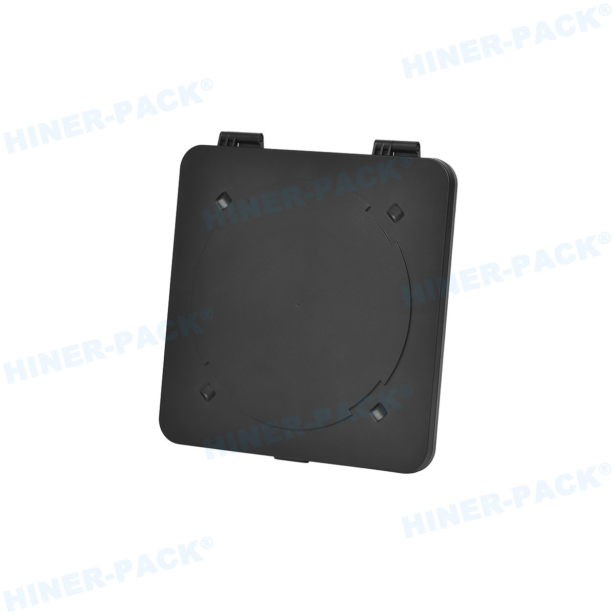
this ecosystem, the wafer box—specifically the
Front Opening Shipping Box (FOSB) for 300mm wafers—serves as the critical
interface between manufacturing sites, outsourcing partners, and final assembly.
Unlike the Front Opening Unified Pod (FOUP) used for in-fab processing, the
wafer box is engineered
for long-duration transport, environmental isolation, and mechanical shock
absorption. As a B2B content strategist specializing in semiconductor materials,
I’ve observed that the transition to 3nm and 2nm nodes has rendered conventional
shipping solutions obsolete. This analysis dissects the engineering imperatives
behind high-performance wafer boxes, integrating data from supply chain audits
and supplier innovations from Hiner-pack,
while mapping actionable procurement strategies for fab operations managers.
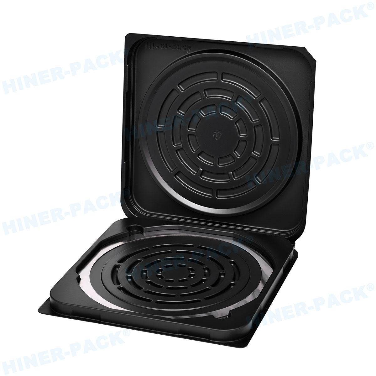
1. Defining the Modern Wafer Box: Beyond Simple Storage
A wafer box in contemporary
semiconductor logistics is a highly engineered microenvironment. Its primary
functions extend far beyond physical protection:
Contamination Barrier: Maintaining internal cleanliness
below ISO Class 1 levels, with particle adders limited to <0.05 particles/cm²
for particles ≥0.1 μm.
Moisture and Gas Control: Utilizing hermetic seals and
desiccant systems to keep relative humidity below 10% and oxygen levels under
0.5% for moisture-sensitive devices.
Mechanical Isolation: Incorporating shock-absorbing
features that dampen vibrations up to 50 G-force impacts during air and ground
transport.
Traceability: Embedded RFID or barcode systems for
real-time inventory tracking across global supply chains.
These requirements are codified in SEMI E47.1 (specifications for FOSBs) and
SEMI E15.1 for equipment interfaces. Non-compliance can result in wafer
breakage, cross-contamination, or electrostatic discharge (ESD) damage, with
each incident potentially costing a fab $100,000 or more in scrapped material
and delayed shipments.
2. Material Science for Transport-Grade Wafer Boxes
While in-fab carriers often use polypropylene (PP) or polycarbonate, the
wafer box for inter-fab
transport demands enhanced material properties to withstand prolonged exposure
to temperature variations (-40°C to 70°C), humidity cycling, and mechanical
stress.
2.1 High-Purity Polypropylene Blends
Advanced wafer boxes utilize impact-modified PP with low ash content
(<0.01%) and minimal oligomer outgassing. These blends must pass SEMI E108
outgassing tests, with total volatile organic compound (TVOC) emissions below
0.1 μg/g. Suppliers now employ supercritical fluid extraction during
manufacturing to eliminate residual mold-release agents that can later migrate
onto wafer surfaces.
2.2 Static-Dissipative Composite Structures
ESD protection remains paramount, especially for devices with gate oxides
thinner than 1.5 nm. Modern wafer boxes integrate carbon nanotube (CNT)-doped
polymers that achieve surface resistivity in the 10³–10⁵ Ω/sq range without
coating delamination. Hiner-pack has pioneered a multi-layer molding process where the inner wafer-contact layer
uses inherently dissipative polymer (IDP) technology, ensuring static decay
times under 0.5 seconds across all humidity levels—a specification increasingly
mandated by logic fabs.
2.3 Anti-Static, Low-Particle Liners
To minimize particle generation from wafer edge contact, some premium wafer
boxes incorporate replaceable foam or elastomer liners. These liners are made
from cross-linked polyethylene with ultra-low particle shedding (<0.01
particles/cm²) and are designed to be swapped after 20–30 transport cycles,
extending the life of the outer shell by 300%.
3. Technical Deep Dive: Contamination Risks in Transit
The most significant yield threats associated with a wafer
box arise during cross-border or inter-facility transit. Three
primary contamination pathways must be addressed:
Airborne Molecular Contamination (AMC): External pollutants
like sulfur dioxide, ammonia, or organic solvents can ingress through imperfect
seals. High-performance wafer boxes employ double-lip silicone gaskets with a
leak rate <0.01 cc/min at 10 psi differential, verified by helium leak
testing per SEMI E49.
Mechanical Abrasion: Vibration during truck or air freight
causes micro-fretting between wafers and box slots. Advanced designs incorporate
radiused slot edges and low-friction coatings that reduce particle generation by
up to 60% compared to standard molded surfaces.
Moisture Ingress: Hydrolytic degradation of packaging
materials can release ionic contaminants. High-end wafer boxes integrate
humidity indicator cards and molecular sieve packs that maintain internal dew
points below -40°C for up to 90 days.
Data from a 2024 supply chain audit revealed that fabs using certified
high-purity wafer boxes experienced 72% fewer contamination-related rejects
during incoming inspection compared to those using non-certified alternatives.
This underscores the economic rationale for investing in premium-grade shipping
solutions.
4. Logistics Integration and Automation Compatibility
Modern semiconductor logistics rely heavily on automated material handling
systems (AMHS) at both sending and receiving fabs. A wafer
box must therefore be compatible with a range of automated
equipment:
Standardized Footprints: Conforming to SEMI E57 kinematic
coupling interfaces for automated load ports.
RFID Read Range: Embedded tags must be readable from
distances of 0.5 to 2 meters to facilitate high-speed sortation in distribution
centers.
Palletization Alignment: Bottom features that securely nest
onto standard 600mm x 800mm semiconductor shipping pallets, preventing shifting
during transit.
Failure to meet these standards disrupts the supply chain. In 2023, a major
OSAT (outsourced semiconductor assembly and test) provider reported a 15%
increase in dock-to-stock cycle time due to incompatible wafer box bases that
caused frequent jams in automated unloading systems. Suppliers like Hiner-pack now offer wafer boxes with precision-molded alignment ribs that ensure seamless
integration with leading automation brands.
5. Total Cost of Ownership (TCO) for Shipping Solutions
Procurement decisions for wafer boxes often focus solely on unit price, but a
TCO analysis reveals a more complex picture. Key TCO drivers include:
Reusability Cycles: Premium wafer boxes engineered with
replaceable wear parts and durable hinges can withstand 50–100 transport cycles,
whereas low-cost alternatives often fail after 20 cycles due to hinge breakage
or seal degradation.
Cleaning Costs: Boxes with non-porous, smooth interior
surfaces reduce cleaning chemical consumption by 30–40% per cycle. Additionally,
validated cleaning protocols (megasonic + DI water rinse) are more effective on
high-purity materials.
Yield Protection: A conservative estimate shows that
switching from standard to advanced ESD-safe wafer boxes reduces defect-related
scrap by 0.15–0.3% for mature nodes and up to 0.5% for advanced
nodes—translating to millions in annual savings for high-volume fabs.
Hiner-pack provides a lifecycle management program that includes periodic recertification
of used boxes, ensuring they meet original cleanliness and ESD specifications.
This circular approach reduces long-term capital expenditure by up to 25% while
maintaining stringent quality standards.
6. Application-Specific Wafer Box Configurations
Different device types and process stages impose unique requirements on the
wafer box. A nuanced
selection process considers these factors:
6.1 MEMS and Sensitive Devices
Micro-electromechanical systems (MEMS) require vibration-dampened boxes with
foam inserts that isolate mechanical shock below 10 G. Specialized wafer boxes
for MEMS also incorporate antistatic foam to prevent charge accumulation on
delicate moving parts.
6.2 High-Value Logic and Memory
For 3nm logic and advanced DRAM, wafer boxes must provide near-hermetic
sealing with integrated getters for moisture and oxygen. Some designs include
pressure-equalization valves that prevent lid popping during air transport while
maintaining contamination control.
6.3 Test and Burn-In Shipping
Wafer boxes destined for test facilities often require thermal stability
features, such as double-wall construction with insulating air gaps, to maintain
wafer temperature uniformity during transport in non-climate-controlled
vehicles.
7. Future Directions: Smart Packaging and Sustainability
The next generation of wafer boxes will
incorporate active monitoring and eco-friendly materials. Key innovations
include:
Embedded IoT Sensors: Real-time monitoring of shock,
temperature, humidity, and even particle counts, with data transmitted via 5G or
LoRaWAN to cloud-based supply chain dashboards. This enables predictive quality
alerts and immediate root-cause analysis for contamination events.
Biobased Polymers: Development of high-purity polymers
derived from renewable feedstocks that meet SEMI cleanliness standards, reducing
the carbon footprint of wafer shipping by an estimated 40% per cycle.
Blockchain-Enabled Traceability: Pairing RFID data with
distributed ledgers to create immutable records of a wafer box’s cleaning
history, transport routes, and contamination test results—a requirement for
automotive and medical device customers.
Industry analysts project that the market for intelligent semiconductor
packaging, including smart wafer boxes, will grow at a CAGR of 12.4% through
2030, driven by the need for supply chain resilience and zero-defect quality
targets in automotive and AI chips.
Frequently Asked Questions (FAQs) on Wafer Box Selection and Management
Q1: What is the primary difference between a FOUP and a wafer box
(FOSB) in semiconductor logistics?
A1: A FOUP
(Front Opening Unified Pod) is intended for in-fab wafer processing and storage,
with features optimized for automated load ports and cleanroom environments. A
wafer box, specifically a FOSB (Front Opening Shipping Box), is designed for
inter-facility transport. FOSBs typically feature enhanced shock absorption,
moisture barrier seals, and durable outer shells to withstand shipping
vibrations and environmental exposure, while FOUPs prioritize low outgassing and
ESD protection for continuous fab use.
Q2: How often should a wafer box be recertified or
replaced?
A2: Recertification frequency depends on
usage and node sensitivity. For leading-edge nodes (5nm and below), wafer boxes
are typically recertified every 20–30 transport cycles or 12 months, whichever
comes first. Recertification includes particle testing per SEMI E47, outgassing
analysis, and ESD verification. High-quality boxes with replaceable liners and
gaskets can achieve 50–80 cycles before retirement, whereas economy versions
often require replacement after 20 cycles due to seal wear or hinge fatigue.
Q3: What certifications should I require when qualifying a wafer box
supplier?
A3: Critical certifications include SEMI
S2 (equipment safety), SEMI S8 (ergonomics), and compliance with SEMI E47.1 for
FOSB specifications. Material certifications must show ICP-MS metal analysis
with <0.01 ppb for 13 critical metals, outgassing reports per SEMI E108 (TVOC
<0.1 μg/g), and ESD verification per SEMI E129 (static decay <2 seconds).
Additionally, ISO 14644-1 Class 1 assembly certification is mandatory for any
wafer box intended for 300mm use.
Q4: Can a wafer box designed for 200mm wafers be used for 300mm
wafers with an adapter?
A4: No, 200mm and 300mm
wafer boxes use entirely different form factors, slot pitches (6.35 mm vs. 10
mm), and interface geometries. Using an adapter is not recommended due to high
risks of wafer slippage, particle generation, and equipment damage. 300mm FOSBs
are standardized for automated load ports, and any deviation can cause tool
jams. Dedicated wafer boxes for each diameter are the only acceptable practice
in high-volume manufacturing.
Q5: How do ESD-safe materials in wafer boxes prevent latent device
failures?
A5: ESD-safe materials with surface
resistivity between 10³ and 10⁵ Ω/sq prevent triboelectric charging during wafer
insertion and removal. Without proper ESD control, static discharge can cause
gate oxide breakdown in advanced FinFET devices, leading to latent failures that
may not manifest until final test. Premium wafer boxes from manufacturers like
Hiner-pack use bulk-dissipative polymers that maintain consistent ESD performance across
varying humidity, protecting devices from both immediate and long-term
reliability issues.
Q6: What is the typical lead time for custom-branded or RFID-enabled
wafer boxes?
A6: For semi-custom modifications such
as company branding, color coding, or RFID integration, lead times range from 6
to 10 weeks, depending on mold availability and validation testing. Full-custom
wafer boxes with unique geometries or material blends require 12–16 weeks for
tooling, SEMI compliance testing, and initial production validation. Suppliers
with pre-qualified modular platforms can reduce lead times by 30–40%.
Q7: Are there recycling programs for end-of-life wafer
boxes?
A7: Yes, several suppliers now offer
take-back programs where wafer boxes are ground, purified, and reprocessed into
non-critical packaging applications. However, due to potential contamination
memory effects, materials from used wafer boxes are generally not recycled back
into high-purity applications for advanced nodes. Sustainable programs focus on
repurposing boxes for non-cleanroom uses or recovering raw materials through
certified waste management partners.
This analysis synthesizes findings
from semiconductor supply chain audits, materials science research, and
collaboration with operations leaders at major foundries and IDMs. For detailed
specifications and qualification support, refer to the Hiner-pack wafer box
series and engage their engineering team for application-specific
guidance.


