In semiconductor manufacturing and advanced wafer-level packaging, the wafer carrier
price is not merely a line item—it directly influences process stability,
defectivity control, and automated material handling system (AMHS)
compatibility. For engineering managers and procurement specialists,
understanding the precise technical parameters that shape carrier pricing is
essential to balance upfront expenditure with long-term reliability. This guide
analyzes material science, industry standards, and real-world application
scenarios to provide a transparent framework for evaluating wafer carrier
investments. Hiner-pack has been a trusted
partner in precision wafer handling solutions, offering engineered carriers that
meet exacting fab requirements without hidden costs.

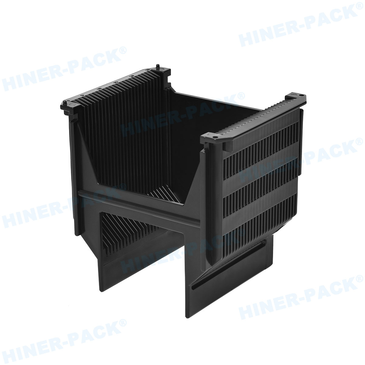
1. Wafer Carrier Typologies and Their Direct Influence on Pricing
Different wafer handling environments demand distinct carrier designs, each
with unique manufacturing complexities that affect the final wafer carrier
price. Below are the primary categories and their cost-relevant
features:
Front Opening Unified Pods (FOUP): Used for 300mm wafer
transport and storage in minienvironments. High-precision injection molding,
anti-static carbon-fiber composites, and integrated RFID tags increase
production costs. Dimensional conformance to SEMI E1.9 and E47.1 requires
post-mold metrology, adding 15–25% to base polymer costs.
Front Opening Shipping Box (FOSB): Similar geometry but
optimized for inter-fab logistics. Requires lower particle shedding and robust
latching mechanisms. Price is driven by material purity and validated
cleanliness (ISO Class 3 or better).
Open Cassettes (Standard Mechanical Interface – SMIF):
Common for 200mm fabs. Lower complexity than FOUPs, yet costs vary with
dimensional stability under thermal cycling (±0.05mm tolerance).
Metal Wafer Carriers (Aluminum/Stainless Steel): For
high-temperature processes (e.g., diffusion, annealing) or harsh chemical
exposure. Precision machining, electropolishing, and passivation layers drive wafer carrier
price significantly higher than polymer options—often 3-5x per unit.
PTFE/PEEK Coated Carriers: Applied in wet etch or plating
tools where chemical resistance is paramount. The coating process and thickness
uniformity control elevate pricing by 40–60% compared to standard polycarbonate
designs.
Each type demands specific mold designs, cleanroom assembly, and quality
validation. For example, a FOUP for 5nm node fabs requires additional outgassing
control (low volatile organic compounds) and surface roughness below 0.4µm Ra,
directly reflected in engineering overheads. Hiner-pack provides
application-specific engineering reports to help customers select the optimal
carrier without overspending on unnecessary specifications.
2. Material Selection: The Primary Determinant of Wafer Carrier Cost
The choice of base polymer or metal alloy dictates mechanical endurance,
electrostatic discharge (ESD) performance, and particle generation. Below are
typical materials and their price implications:
Polycarbonate (PC): Baseline material for open cassettes
and some FOSBs. Low cost, but limited chemical resistance and higher moisture
absorption. Price-sensitive projects often start here.
Polyetheretherketone (PEEK): Superior thermal stability (up
to 260°C), exceptional chemical resistance, and low outgassing. PEEK resin
prices are 8–10x higher than PC. Carriers for high-temperature SiC or GaN
processes almost exclusively use PEEK, raising wafer carrier
price substantially but reducing replacement frequency.
Polyethersulfone (PES): Transparent amber material with
good heat deflection (210°C). Often used in FOUP windows or inspection carriers.
Cost lies between PC and PEEK.
Carbon-fiber reinforced composites: Added to PC or PEEK to
lower surface resistivity (10^3–10^5 Ω/sq) for ESD-safe handling. The
compounding process and fiber dispersion quality increase material cost by
30–50%.
Stainless Steel 316L: Used for fully-automated wet
stations. High-density machining, electropolishing to Ra ≤0.2µm, and passivation
per ASTM A967 add considerable fabrication expenses.
Beyond raw materials, the injection molding process for large 300mm carriers
requires multi-ton clamping forces and precision temperature control. Defect
rates (warpage, sink marks, or flash) can reach 5-8% for complex designs, and
those costs are absorbed into per-unit pricing. Industry data suggests that
carriers requiring class 1 cleanroom assembly and double-bagging in anti-static
films add $12–$18 per unit in logistics overhead.
3. Industry Pain Points: Why Low-Cost Carriers Often Lead to Higher
Defectivity and Tool Wear
Procurement teams under pressure to minimize upfront spending frequently
encounter reliability issues that erode fab efficiency. Below are documented
pain points from high-volume manufacturing environments:
Uncontrolled particle shedding: Non-certified carriers can
generate >200 particles/m³ (>0.1µm), directly impacting yield in gate
oxide or photolithography steps. Replacing a single contaminated lot costs
exponentially more than investing in quality carriers.
Dimensional drift after thermal cycling: FOUPs for post-CMP
or annealing see 50–70°C variations. Poorly molded polymer carriers exhibit
warpage >0.2mm, leading to robot arm misalignment and wafer edge damage. Each
robot recalibration costs upwards of $2,000 in technician time.
ESD failures in sensitive devices: Carriers without
controlled resistivity (10^5–10^11 Ω/sq) accumulate charge, causing gate oxide
breakdown. The average ESD-related loss in a 300mm fab is estimated at 1.5–2% of
total wafer output.
Incompatibility with SEMI standards: Non-compliant carriers
cause AMHS jams, resulting in line stoppages. Downtime for a 300mm line is
valued at $30,000–$50,000 per hour.
These issues underscore that evaluating a wafer carrier
price in isolation ignores hidden operational risks. A systematic approach
factoring particle performance, metrology certification, and supplier audit
evidence is more cost-effective. Hiner-pack supplies lot-specific
inspection reports including dimensional measurement and particle count data,
aligning with ISO 14644-1 cleanroom standards.
4. Strategies to Optimize Wafer Carrier Procurement and Reduce Total
Risk
Leading fabs and OSATs employ several methods to rationalize spending without
compromising process integrity:
Standardized carrier pools: Using a unified design across
multiple process steps reduces inventory variety and simplifies requalification.
For example, adopting a single FOUP model for both etch and metrology sections
cuts qualification efforts by 40%.
Supplier early engagement: Involving carrier manufacturers
during tool layout planning allows optimization of door mechanisms, kinematic
coupling pins, and mapping slot accuracy. This avoids costly post-production
modifications.
Reclamation and recertification programs: Many carriers can
be cleaned, refurbished, and re-certified after 2-3 years of use, offering
40-60% savings compared to new units. Ensure the supplier follows a documented
recertification protocol (visual inspection, particle measurement, ESD
verification).
Volume commitment agreements: Committing to annual volumes
of 5,000+ units allows tiered pricing and just-in-time delivery schedules.
Negotiate for mold amortization to be spread over multiple years.
Material upgrade only where necessary: Use PEEK carriers
only in high-temperature or aggressive chemical modules (e.g., photoresist
stripping). For ambient storage and standard transport, advanced PC or PES
blends provide adequate performance at lower wafer carrier
price.
Adopting these strategies requires transparent technical documentation from
the vendor. Hiner-pack provides full
material datasheets, SEMI compliance certificates, and sample testing kits to
validate carrier performance before volume procurement.
5. Application-Driven Price Scenarios in Advanced Packaging
Wafer carriers are not limited to front-end fabs; advanced packaging flows
such as fan-out wafer-level packaging (FOWLP), 3D IC stacking, and hybrid
bonding introduce specific handling demands that affect pricing structures.
Thin wafer handling (50–150µm thickness): Temporary bonding
to glass or silicon carriers requires ultra-flat surfaces (<10µm TIR). These
specialized carriers undergo double-side polishing and edge rounding, raising
per-unit cost by 100–150% compared to standard thickness carriers.
Carrier rings for tape expansion: In die sorting and sawing
processes, stainless steel or carbon-fiber rings need precise flatness and
magnetic properties. Laser-cut and stress-relieved rings command premium pricing
but prevent warpage during thermal die attach.
High-temperature glass carriers: For panel-level packaging
(PLP), borosilicate glass carriers withstand 600°C+ processes. Their price is
driven by defect-free surface quality and coefficient of thermal expansion
matching silicon.
Anti-bonding carriers with micro-structures: Some advanced
packaging uses temporary bonding adhesives; carriers with micro-grooves or
release layers simplify debonding. Photolithography-defined patterns increase
fabrication complexity and cost.
Each scenario shows that the wafer carrier
price must be analyzed within the specific toolset and process window. A
carrier that is over-engineered for passive storage will waste budget, while an
under-engineered carrier for thin-wafer handling will cause breakage rates as
high as 5% per lot.
6. Market Trends Impacting Wafer Carrier Costs Through 2026
Several industry shifts are reshaping supply chains and price structures for
wafer handling products:
Reshoring of semiconductor supply chains: Regional fabs in
North America and Europe are demanding local carrier production, shortening lead
times but potentially increasing unit costs by 10–15% compared to Asian mass
production. However, reduced logistics risk and faster engineering support
provide offsetting benefits.
Adoption of recycled and bio-based polymers: Pilot projects
using post-consumer recycled PC for non-critical cassettes have shown 20% lower
material costs, pending qualification for particle performance. Broader adoption
may soften price increases.
Automated optical inspection (AOI) integration: In-line
carrier inspection tools (laser profilometry, surface scanners) are becoming
standard. Vendors investing in AOI pass cost to pricing, but lower defect
returns offset the premium over 2-3 years.
Customization for 200mm legacy fabs: As many mature nodes
remain active (automotive, power ICs), demand for 200mm carriers with modern ESD
and low-particle designs is rising, stabilizing prices for these formats despite
lower overall volume.
Staying informed of these trends helps procurement teams time purchases and
negotiate better terms. For real-time wafer carrier
price benchmarks, Hiner-pack offers a quarterly
pricing index based on material futures and cleanroom labor rates, available to
qualified buyers.
Frequently Asked Questions (FAQ) – Wafer Carrier Pricing and Selection
Q1: Why is the wafer carrier price for 300mm FOUPs significantly
higher than 200mm open cassettes?
A1: 300mm FOUPs require much
tighter dimensional tolerances (≤0.1mm across 450mm length), integrated ESD-safe
door mechanisms, and compatibility with SMIF (Standard Mechanical Interface)
load ports. The injection molding tools are larger and demand higher clamping
forces (up to 2,000 tons), and each FOUP undergoes individual particle
certification (ISO Class 3). Conversely, 200mm open cassettes have simpler
geometry, fewer moving parts, and can be molded in multi-cavity tools, reducing
per-unit costs by 40–50%.
Q2: How do I compare wafer carrier price quotes from different
suppliers if specifications vary?
A2: Request a standardized data
sheet including: material grade and supplier, surface resistivity range,
outgassing test results (by GC-MS), dimensional report per SEMI E15.1, and
cleanroom assembly grade (ISO 5 or better). Also ask for included accessories
(e.g., RFID tags, shipping covers, sealing films). Normalize quotes by factoring
mold amortization, minimum order quantity, and recertification services.
Hiner-pack provides a free
comparison template to ensure you are comparing equivalent specifications.
Q3: Can I receive samples or small batches before committing to a
volume order?
A3: Yes, most specialized carriers—especially PEEK or
carbon-fiber reinforced types—require process validation. Reputable vendors
offer engineering sample lots (5–25 units) with a partial mold fee that is
refundable upon volume commitment. The sample wafer carrier
price per unit is typically 30–40% higher than production pricing due to
setup costs, but this allows you to run reliability tests (thermal cycling,
particle monitoring, robot compatibility). Always request a sample qualification
plan before approving final pricing.
Q4: Does a higher wafer carrier price always mean better long-term
performance?
A4: Not automatically. Some premium-priced carriers
include unnecessary features such as exotic coatings for ambient processes.
Evaluate the correlation between price and critical parameters: for etch
modules, chemical resistance is key; for lithography, low outgassing and smooth
surface finish matter more. Obtain life-test data (e.g., 10,000 insertion cycles
with particle trend analysis). A moderately priced carrier from a qualified
supplier often outperforms a high-cost but poorly documented alternative. Focus
on SEMI-certified options with third-party validation.
Q5: How does the order volume affect wafer carrier price per
unit?
A5: Volume significantly influences unit economics due to mold
amortization and batch cleaning costs. For injection-molded carriers, tooling
can range from $15,000 (simple cassette) to $120,000 (complex FOUP). At 500
units/year, mold cost adds $30–$240 per unit; at 10,000 units/year, that drops
to $1.5–$12 per unit. Additionally, cleanroom packing and particle sampling have
fixed batch setup costs. For annual volumes above 5,000 units, negotiate a
tiered price schedule and consider consignment inventory to reduce your holding
expenses.
Q6: What certifications should I require to ensure my wafer carrier
price reflects genuine quality?
A6: Always mandate SEMI E1.9
(specifications for 300mm FOUPs), SEMI E15.1 (measurement methods), and
optionally SEMI S2 (environmental safety). For cleanroom use, ask for ISO
14644-1 Class 3 or better particle count per carrier. ESD performance should
follow ANSI/ESD S20.20 compliance. A transparent supplier will provide
batch-specific certificates of analysis (CoA) including surface roughness,
outgassing (VOC) levels, and flatness measurements. Any supplier unwilling to
share this data likely hides process inconsistencies.
Need an accurate,
specification-based quotation for your fab’s wafer handling requirements? Our
engineering team at Hiner-pack provides detailed
proposals including material recommendations, SEMI compliance documentation, and
life-cycle cost projections. Send your inquiry now to receive a
customized wafer carrier
price assessment within 48 hours, along with sample qualification support.
Click here to start your inquiry
→


