For semiconductor packaging and wafer-level processing, the carrier that
transports, stores, and protects silicon wafers is not a commodity. A precise
wafer carrier
quotation involves much more than a base price — it reflects
material science decisions, contamination control strategies, cleanroom
logistics, and process-specific engineering trade-offs. Procurement and process
engineers who treat carrier quotes as simple unit-price comparisons often
encounter yield issues, particle contamination, or dimensional mismatches later
in production. This article provides a deep, criteria-based walkthrough for
obtaining and evaluating wafer carrier
quotation documents, with emphasis on key performance indicators
that directly affect front-end and back-end fabs.
Core Factors That Shape a Wafer Carrier Quotation
When you request a wafer carrier
quotation from any supplier, the line items should reflect the
following engineering-driven components. Failing to specify these details leads
to ambiguous pricing and potentially incompatible carriers.
1. Base Polymer & ESD Formulation
Carriers are injection-molded from materials such as polycarbonate (PC),
polyetheretherketone (PEEK), or polyetherimide (PEI). The resin type plus
static-dissipative fillers (carbon fiber, conductive polymers, or anti-static
agents) directly influence cost. Surface resistivity must typically fall between
10³ and 10⁶ Ω/sq for 300mm FOUP and FOSB applications. For high-temperature
curing steps (200–250°C), PEEK-based carriers are mandatory but increase the
quote by 40–60% compared to PC. The quote should clearly state the material
grade, ASTM E595 outgassing test compliance (if needed), and surface resistivity
range per SEMI E78.
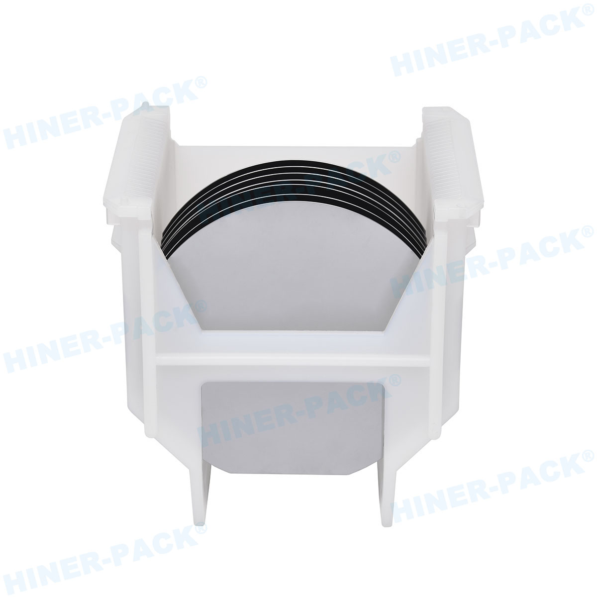
2. Dimensional Specifications & Metrology Requirements
Carrier geometry includes slot pitch, wafer pocket depth, protrusion control,
and flatness across the base plate. For automated wafer handling equipment,
total run-out and slot parallelism tolerances are often ±0.05 mm. Non-standard
wafer thicknesses (e.g., thin wafers after backgrinding) require custom pocket
designs, which involve NRE (non-recurring engineering) costs — this must be
separately detailed in any wafer carrier
quotation. Always request metrology reports with Cpk values (≥1.33)
for critical dimensions.
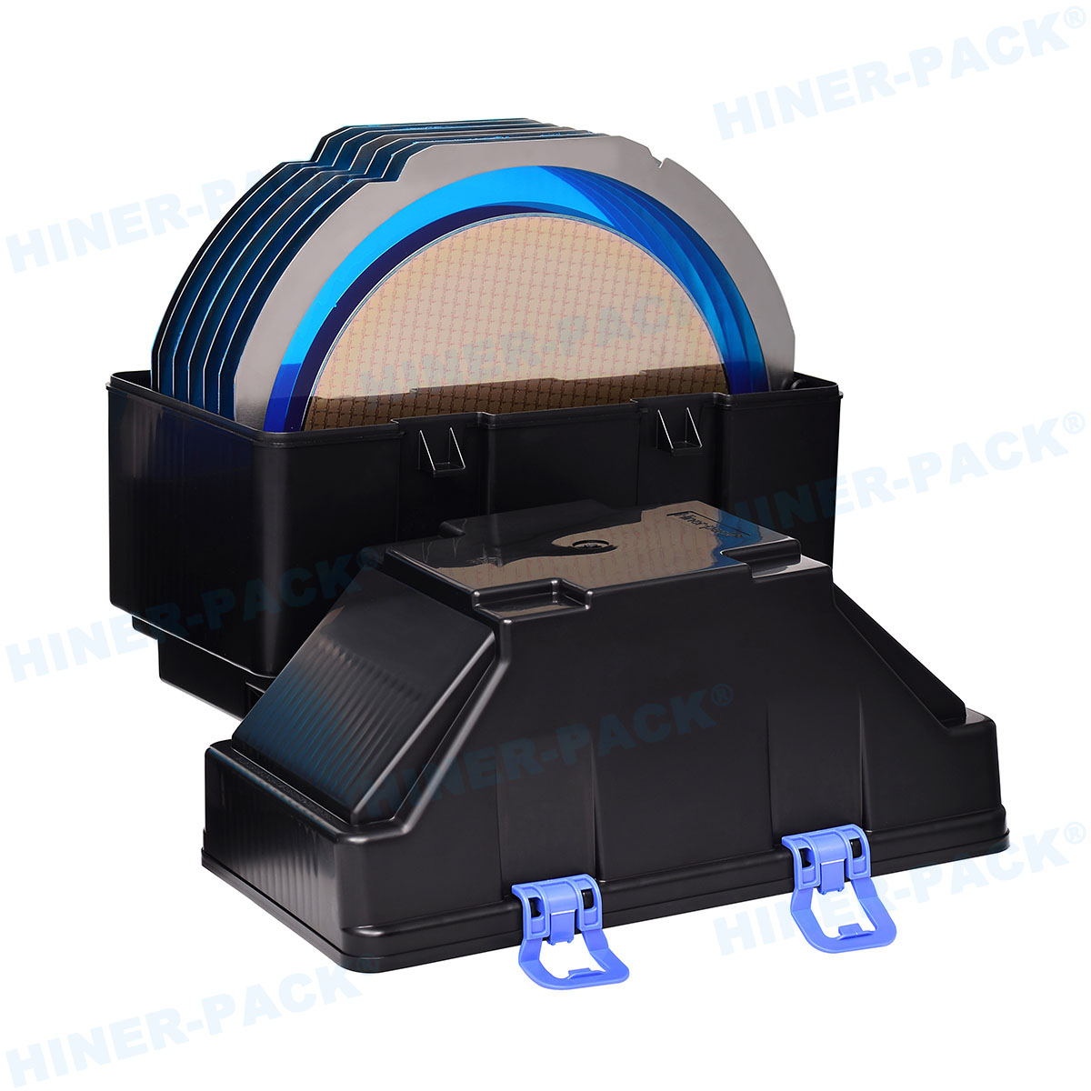
3. Cleanroom Packaging & Certification Level
After molding, carriers are cleaned in deionized water, dried in laminar flow
ovens, and double-bagged in Class 10/ISO 4 cleanroom environments. Some
processes require individual nitrogen-purged bags or ESD-safe vacuum packaging.
Each level of post-molding processing adds operational steps and consumables,
reflected in the quote’s per-unit handling fee. Ask for a breakdown of packaging
certification compliance (ISO 14644-1 Class 4 or better).
4. Tooling and Customization NRE
If your application requires a non-SEMI-standard carrier (e.g., special
keying, RFID slots, or modified notch alignment), the supplier must design and
fabricate new injection molds. The mold cost amortization should be transparent:
either as a one-time NRE line item or spread over an agreed order volume.
Standard carriers (SEMI E1.9 compliant for 150mm/200mm) have zero NRE. For
custom designs, tooling typically ranges from $8,000 to $35,000 depending on
complexity and number of cavities.
5. Order Quantity and Lead-Time Flexibility
Low-volume prototyping (25–100 units) commands a higher per-part price due to
machine setup, material batch costs, and manual inspection. Volume pricing
starts from 500 units upward, with additional discounts at 2,000+ units. Rushed
orders (≤15 business days) often include a 25–40% expediting premium. A robust
wafer carrier quotation will offer tiered pricing based on
annual volume forecasts.
How to Request an Actionable Wafer Carrier Quotation: Step-by-Step
To avoid vague estimates and back-and-forth delays, structure your RFQ
(request for quotation) with the following mandatory parameters. Suppliers with
deep packaging expertise — such as Hiner-pack — can transform this
data into a firm, engineering-backed quotation within 3–5 business days.
Wafer dimensions: diameter (150mm, 200mm, 300mm), thickness
range (pre-grind and final thickness if different).
Carrier type: FOUP (front opening unified pod), FOSB (front
opening shipping box), SMIF pod, or open cassette. Specify if automated or
manual loading.
Material electrical properties: required surface
resistivity range and whether carbon fiber shedding is allowed (low-shedding for
sensitive devices).
Thermal and chemical exposure: maximum operating
temperature, exposure to acids/solvents (e.g., clean cycles with isopropyl
alcohol).
Handling interface: robot end-effector clearances, bottom
flange dimensions (for automated guided vehicles).
Cleanliness grade: particle specification ≤0.1 μm per SEMI
E62; also specify outgassing limits for non-volatile residues.
Include drawings or 3D step files for custom designs. Experienced vendors
like Hiner-pack provide a detailed
response including material certificates, dimensional inspection methods, and
prototype sampling lead times.
Material Choices and Their Influence on Quoted Pricing – An Engineering
Deep-Dive
Semiconductor wafer carriers must balance mechanical strength, electrostatic
discharge (ESD) control, thermal stability, and chemical resistance. Below is a
comparative analysis of the three dominant resin systems and their effect on a
wafer carrier quotation.
Antistatic Polycarbonate (PC) – Workhorse for Standard Processes
Most 200mm and some 300mm carriers use antistatic PC (filled with conductive
carbon or permanent antistatic agents). Advantages: good impact resistance, low
moisture absorption, moderate cost. Surface resistivity stabilized between
10⁵–10⁷ Ω/sq. Temperature limit: 120°C continuous use, 140°C intermittent. PC
carriers are suitable for die-attach, wire bonding, and final test environments
not exceeding 125°C. A typical injection-molded antistatic PC carrier for 200mm
wafers has a unit price range of $45–$90 in volumes of 500 units, with tooling
NRE between $5k–$12k. However, for high-temperature processes like polyimide
curing or wafer-level molding (>150°C), PC carriers warp and outgas, leading
to wafer scrapping.
High-Performance PEEK – For Harsh Thermal and Chemical Environments
PEEK (polyetheretherketone) carriers resist continuous 250°C exposure,
withstand aggressive solvents (acetone, NMP, sulfuric acid) and produce
extremely low particles. The filler system for ESD compliance uses carbon fiber
or carbon nanotubes, achieving resistivity 10⁴–10⁶ Ω/sq consistently. The
downsides: injection molding requires higher melt temperatures (350–390°C) and
tool steel grade, plus longer cycle times. Consequently, a PEEK wafer carrier
for 300mm applications starts at $280–$500 per unit in moderate volumes. Tooling
costs are also higher — typically $18,000–$38,000 due to corrosion-resistant
molds. A wafer carrier quotation for PEEK should always include
detailed flow simulation and warpage analysis because PEEK shrinkage behaves
differently than PC.
Conductive PEI (Ultem) – Balanced Option for Specific Workflows
Polyetherimide (branded as Ultem) offers higher heat deflection (210°C
continuous) and inherent flame resistance without halogens. Conductive grades
(using carbon powder) maintain resistivity in the 10⁶–10⁹ Ω/sq range, suitable
for less sensitive ESD environments. PEI has lower outgassing compared to PC,
and its chemical resistance is good for most fab cleaning cycles. Cost falls
between PC and PEEK: $150–$220 per carrier for 300mm size. The wafer
carrier quotation for PEI may also require annealing steps after
molding to relieve internal stress, which affects delivery lead times.
When requesting pricing, always ask for the supplier’s control plan regarding
filler dispersion: uneven conductive filler distribution creates “hot spots”
(low resistivity) or insulating zones (high surface voltage). Leading suppliers
such as Hiner-pack implement statistical
process control (SPC) on injection parameters to guarantee homogeneity.
Evaluating Multi-Vendor Wafer Carrier Quotations: Pitfalls and Critical
Checks
Receiving three different wafer carrier quotation documents
from different suppliers can be confusing if they use dissimilar cost
structures. Use the following matrix to compare beyond unit price.
Lifecycle cost of cleanroom requalification: Some suppliers
provide cheaper carriers but skip post-mold cleaning and particle testing. This
forces the buyer to perform additional cleaning, adding $10–$20 per
carrier.
Dimensional repeatability across production batches: Demand
historical capability data (Cpk on slot width, pitch, and coplanarity). A
lower-priced supplier may have wider control limits (Cpk <1.0), causing robot
end-effector crashes.
Material traceability: Does the quote include batch-level
lot control and resin certificates of analysis? High-quality quotes always list
resin supplier name and filler type.
Warranty for ESD property degradation: After 100+ cleaning
cycles, antistatic properties can decay due to surfactant washout. A robust
quotation should mention ESD retention test data per SEMI E78.
Sample approval process: Does the supplier provide
engineering samples (5–20 pcs) for qualification before mass production? The
sample cost should be clearly stated or waved against first order.
For advanced packaging processes such as fan-out wafer-level packaging
(FOWLP) where wafer bow is significant, the carrier must accommodate non-planar
wafers. In such cases, request the quote to include finite element analysis
(FEA) of stress distribution on the wafer edge – a mark of a true
engineering-driven supplier.
Streamlining Wafer Carrier Procurement with Hiner-pack
Over the past decade, Hiner-pack has established
itself as a specialized provider of injection-molded carriers for 100mm to 300mm
wafer processing. Their approach to a wafer carrier quotation integrates each of the above factors — material traceability, ESD stability,
cleanroom packaging, and clear NRE amortization. When you upload your wafer
geometry and process environment to their platform, the engineering team returns
a detailed breakdown with lead times, sampling plan, and SPC commitment. For
fabs looking to consolidate suppliers and reduce qualification risk, Hiner-pack
provides consistent quality across multiple facilities. Visit their carrier
series page for direct access to standard and custom models.
Frequently Asked Questions (FAQ) – Wafer Carrier Quotation
Q1: What documents should I attach to get an accurate wafer carrier
quotation for a non-standard wafer thickness?
A1: Provide a detailed mechanical drawing indicating wafer diameter, thickness
(including tolerances), notch/flat orientation, and any special pocket
clearances. Also specify the material resistivity requirement and maximum
process temperature. Suppliers like Hiner-pack use this data to simulate molding
and will include NRE and per-part pricing in the wafer carrier
quotation.
Q2: How do I verify if a quoted carrier meets particle emission
standards for a Class 1 cleanroom?
A2: Request that
the supplier include particle test results per SEMI E62 (liquid particle count
after ultrasonic extraction) as part of the quotation. Acceptable levels are ≤10
particles >0.1μm per cm². Leading suppliers incorporate these tests into
their outgoing quality control and will attach a certificate with each shipment
batch.
Q3: Can a wafer carrier quotation include an option for RFID tags or
smart tracking features?
A3: Yes. Many advanced
fabs require RFID pockets or pre-installed passive tags. The quote should list
the type of RFID insert (e.g., 13.56 MHz or UHF), its protective encapsulation,
and any extra molding operations to embed the tag. This typically adds $5–$12
per carrier plus a one-time encoder purchase if needed.
Q4: What typical lead time should I expect from quotation to
delivered carriers for a custom design?
A4: For a
completely new injection mold, tooling fabrication takes 6–9 weeks. First
articles (25 units) are shipped another 2 weeks after tool approval. For
semi-custom designs (minor modifications to existing mold platforms), lead times
shrink to 4–5 weeks for engineering samples. Volume production follows 3–4 weeks
after sample approval. Always confirm these lead times are listed in the
wafer carrier quotation to avoid schedule surprises.
Q5: Does Hiner-pack provide free engineering samples for evaluation
before mass production?
A5: For qualified
semiconductor accounts with a projected annual volume above 1,000 units,
Hiner-pack often provides first-article samples at no additional cost (excluding
shipping). For low-volume or first-time collaborations, sample costs are shared
but are deducted from the first production order. Consult their sales team
through the website for specific sample policies.
Q6: How does the surface finish of a carrier influence wafer scratch
risk, and is it reflected in the quotation?
A6: Smoothness of pocket ribs and wafer contact points directly relates to defect
rates. A comprehensive quotation includes surface roughness data (Ra ≤0.8μm for
critical contact areas). Advanced quotes also mention mold polishing method
(spark erosion, diamond polishing). If not mentioned, specifically request this
data before order confirmation.
Q7: What is the typical minimum order quantity (MOQ) for a custom
ESD-safe PEEK carrier?
A7: Due to high material
cost and specialized molding, MOQ for PEEK carriers is commonly 100 units.
However, some suppliers accept 50-unit pilot runs at a higher per-unit
multiplier (20–35% premium). This should be clearly identified in the
wafer carrier quotation to align with your development
budget.
Ready to Get a Precise Wafer Carrier Quotation for Your Fab?
Engineering-grade wafer carriers directly influence process yield, tool
uptime, and contamination control. Avoid generic estimates by sending your
technical requirements to a supplier that understands semiconductor-grade
injection molding. Whether you need antistatic PC for assembly, PEEK for
high-temperature curing, or custom-designed carriers with RFID integration,
initiate your inquiry by providing detailed specifications. Use the form below
or contact directly via the provided channels to receive a comprehensive,
line-item quotation within 72 business hours.
Send
your wafer carrier inquiry now:
Email:rainbowzhu@hiner-pack.com(please include CAD files if available)
Online form: https://www.waferboxes.com/contact
Mandatory information: wafer size, material resistivity requirement, operating
temperature, estimated annual volume.
All quotation requests receive
a technical review by packaging engineers, not sales generalists.
For direct access to standard carrier families (200mm FOUP, 300mm FOSB, SMIF
pods), browse the product catalog at Hiner-pack. Their published lead
times and specification sheets allow quick reference before requesting a formal
wafer carrier
quotation. Optimize your carrier supply chain with engineering
transparency and manufacturing consistency.


