
In the highly precise world of semiconductor production, every component plays a critical role in ensuring the integrity and efficiency of the manufacturing process. Among these, wafer carriers stand out as essential tools for handling and transporting silicon wafers—the foundational elements of modern electronics. As the demand for smaller, faster, and more powerful devices grows, the importance of reliable wafer carriers semiconductor solutions cannot be overstated. This article delves into the multifaceted aspects of wafer carriers, covering everything from selecting the right wafer carrier semiconductor manufacturer to understanding custom wafer carrier semiconductor options, effective wafer carrier semiconductor cleaning protocols, and detailed wafer carrier technical specifications. By exploring these areas, we aim to provide a comprehensive resource for professionals in the industry, helping them optimize their operations and maintain high standards of quality and safety.
The Critical Role of Wafer Carriers in Semiconductor Production
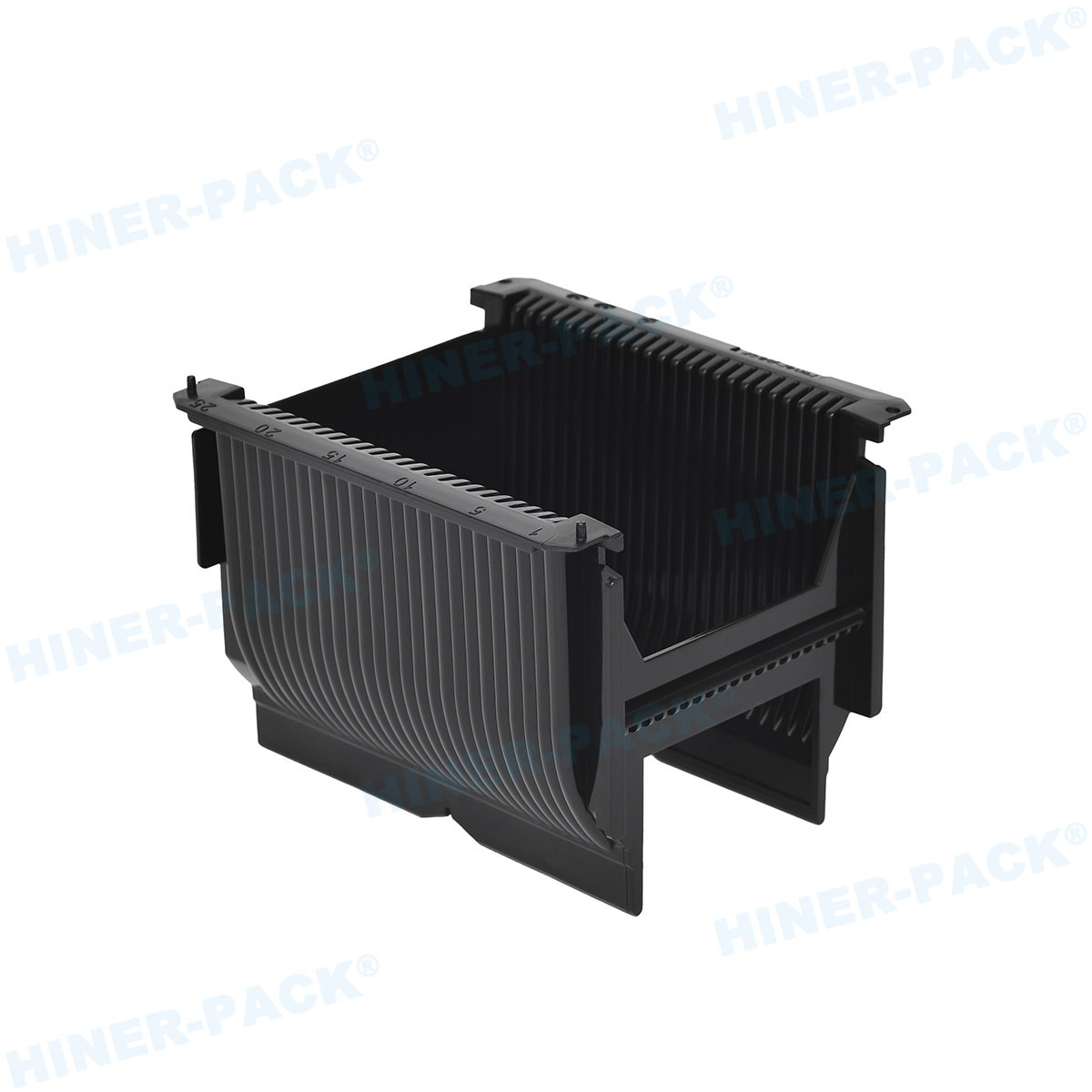
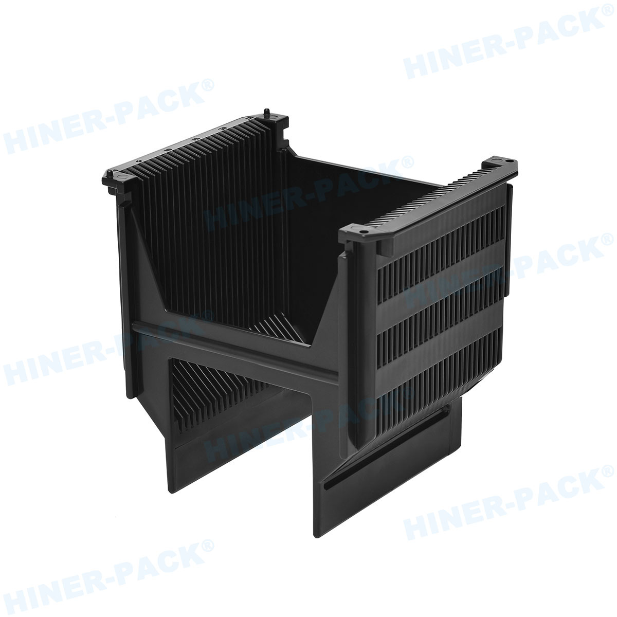
Wafer carriers, also known as wafer cassettes or pods, are specialized containers designed to hold and protect silicon wafers during various stages of semiconductor fabrication. These stages include lithography, etching, doping, and packaging, where even minor contaminants or physical damage can lead to significant yield losses. The primary function of a wafer carrier is to safeguard wafers from environmental factors such as dust, moisture, and static electricity, while also facilitating automated handling in cleanroom environments. Given the delicate nature of wafers—often as thin as a human hair and susceptible to micro-fractures—the design and material of wafer carriers must meet stringent requirements. In the broader context of the semiconductor industry, wafer carriers semiconductor components are integral to maintaining throughput and minimizing defects. As technology advances toward smaller nodes (e.g., 5nm and below), the specifications for these carriers become even more demanding, driving innovation in materials and design. This section sets the stage for a deeper look into the key elements that define modern wafer carrier solutions, including manufacturing, customization, cleaning, and technical details.
Choosing the Right Wafer Carrier Semiconductor Manufacturer
Selecting a reputable wafer carrier semiconductor manufacturer is a crucial decision for any semiconductor fabrication facility (fab). A reliable manufacturer not only ensures high-quality products but also provides support in terms of customization, compliance with industry standards, and after-sales service. The best manufacturers typically have extensive experience in the semiconductor sector, with certifications such as ISO 14644 for cleanroom compatibility and SEMI standards for material purity. When evaluating a wafer carrier semiconductor manufacturer, consider factors like their production capabilities, material selection, and ability to scale with your needs. For instance, leading manufacturers often use advanced polymers like perfluoroalkoxy (PFA) or polyetheretherketone (PEEK), which offer excellent chemical resistance and low particulate generation. Additionally, they may employ injection molding or machining techniques to achieve precise tolerances, critical for maintaining wafer integrity. Collaboration with a trusted wafer carrier semiconductor manufacturer can also lead to innovations in carrier design, such as anti-static features or ergonomic handles for easier manual handling. In summary, partnering with a top-tier wafer carrier semiconductor manufacturer is essential for achieving consistent performance, reducing contamination risks, and ultimately enhancing yield in semiconductor production lines.
The Advantages of Custom Wafer Carrier Semiconductor Solutions
In many cases, off-the-shelf wafer carriers may not fully address the unique requirements of a specific semiconductor process. This is where custom wafer carrier semiconductor options come into play, offering tailored solutions that optimize performance and efficiency. Customization can involve adjustments in size, shape, material, or additional features like RFID tagging for traceability or integrated sensors for environmental monitoring. For example, a fab working with larger 450mm wafers might need carriers with enhanced structural support to prevent warping, while those in high-temperature processes may require materials with superior thermal stability. The process of developing a custom wafer carrier semiconductor solution typically begins with a detailed assessment of the application needs, followed by prototyping and testing to ensure compatibility. Working closely with a manufacturer experienced in custom wafer carrier semiconductor projects allows for iterative improvements, reducing the risk of failures in production. Beyond functional benefits, custom solutions can also lead to cost savings by minimizing waste and improving workflow integration. As semiconductor technologies evolve, the demand for custom wafer carrier semiconductor products is expected to rise, driven by the need for greater precision and adaptability in advanced manufacturing environments.
Essential Practices for Wafer Carrier Semiconductor Cleaning
Maintaining the cleanliness of wafer carriers is paramount in semiconductor manufacturing, as even microscopic contaminants can cause defects in wafers, leading to costly rework or scrap. Effective wafer carrier semiconductor cleaning protocols are designed to remove residues, particles, and electrostatic charges without damaging the carrier itself. Common cleaning methods include ultrasonic baths with deionized water, chemical cleaning using solvents like isopropyl alcohol, and plasma cleaning for removing organic contaminants. The frequency and intensity of wafer carrier semiconductor cleaning depend on the specific process; for instance, carriers used in deposition steps may require more frequent cleaning due to buildup of thin films. It's also important to follow standardized procedures, such as those outlined in SEMI E108 for carrier maintenance, to ensure consistency. Automated cleaning systems are increasingly popular in high-volume fabs, as they reduce human error and enhance throughput. Additionally, proper storage of cleaned carriers in controlled environments prevents recontamination. By implementing rigorous wafer carrier semiconductor cleaning routines, facilities can extend the lifespan of their carriers, maintain high yield rates, and comply with industry regulations for particulate control. This proactive approach is a key aspect of overall contamination management in semiconductor production.
Understanding Wafer Carrier Technical Specifications
When selecting or designing wafer carriers, a thorough understanding of wafer carrier technical specifications is essential to ensure compatibility with existing equipment and processes. These specifications cover a range of parameters, including dimensional tolerances, material properties, and performance metrics. Key wafer carrier technical specifications often include internal dimensions to accommodate specific wafer sizes (e.g., 200mm, 300mm, or 450mm), slot pitch for wafer spacing, and overall weight for handling considerations. Material specifications might detail the type of polymer used, its purity level, and resistance to chemicals like acids or bases. Other critical aspects include static dissipation properties to prevent electrostatic discharge (ESD), thermal expansion coefficients for high-temperature applications, and load capacity for robotic automation. Standards such as SEMI E1.9 for 300mm carriers provide guidelines for interoperability, ensuring that carriers from different manufacturers can be used interchangeably in automated systems. Additionally, wafer carrier technical specifications may include certifications for cleanroom use, such as low particle emission rates. By carefully reviewing these specs, engineers can make informed decisions that align with their production goals, reduce downtime, and enhance overall efficiency. As the semiconductor industry pushes toward more complex architectures, the evolution of wafer carrier technical specifications will continue to play a vital role in supporting next-generation technologies.
The Future of Wafer Carriers in Semiconductor Innovation
The semiconductor industry is in a constant state of evolution, driven by trends like the Internet of Things (IoT), artificial intelligence (AI), and 5G connectivity. These advancements place increasing demands on wafer carriers semiconductor components, necessitating continuous improvements in design, materials, and functionality. Future developments may include smart wafer carriers equipped with IoT sensors for real-time monitoring of temperature, humidity, and contamination levels, enabling predictive maintenance and data-driven optimization. Sustainability is another growing focus, with manufacturers exploring recyclable materials and energy-efficient production methods for wafer carriers. Moreover, as wafer sizes potentially increase beyond 450mm, carriers will need to address challenges related to weight distribution and mechanical stability. Collaboration across the supply chain—from wafer carrier semiconductor manufacturer to end-users—will be crucial in driving these innovations. By staying abreast of emerging trends and investing in R&D, the industry can ensure that wafer carriers remain a reliable backbone of semiconductor manufacturing, supporting the creation of faster, more efficient electronic devices for years to come.
Frequently Asked Questions About Wafer Carriers in Semiconductor
Q1: What is the primary purpose of a wafer carrier in semiconductor manufacturing?
A1: The primary purpose of a wafer carrier is to safely hold, transport, and protect silicon wafers during the semiconductor fabrication process. It prevents contamination, physical damage, and electrostatic discharge, ensuring high yield and quality in production lines.
Q2: How do I choose a reliable wafer carrier semiconductor manufacturer?
A2: When selecting a wafer carrier semiconductor manufacturer, consider their industry experience, certifications (e.g., ISO standards), material quality, and ability to provide custom solutions. Look for manufacturers with a proven track record in semiconductor applications and positive customer reviews.
Q3: What are the benefits of opting for a custom wafer carrier semiconductor solution?
A3: Custom wafer carrier semiconductor solutions offer tailored designs to meet specific process requirements, such as unique wafer sizes, enhanced durability, or integrated features like tracking systems. This can lead to improved efficiency, reduced contamination, and better compatibility with automated equipment.
Q4: Why is wafer carrier semiconductor cleaning so important, and how often should it be done?
A4: Wafer carrier semiconductor cleaning is critical to remove contaminants that could cause defects in wafers. The frequency depends on the process; for high-contamination steps, cleaning might be needed after each use, while less critical applications may allow for weekly or monthly cycles. Always follow manufacturer guidelines and industry standards.
Q5: What key specifications should I review in wafer carrier technical specifications?
A5: Important wafer carrier technical specifications include dimensional accuracy (e.g., slot width and depth), material type and purity, static dissipation properties, thermal resistance, and compliance with industry standards like SEMI. These ensure the carrier functions effectively in your specific environment.
By addressing these common questions, we hope to clarify the essential aspects of wafer carriers in the semiconductor industry, aiding in informed decision-making and optimal operational practices.


