In the highly precise world of semiconductor manufacturing, every component plays a critical role in ensuring the integrity and yield of microchips. Among these, the silicon wafer container stands out as an essential element that safeguards delicate silicon wafers throughout their journey from production to assembly. As the backbone of wafer handling and storage, understanding the silicon wafer container is vital for anyone involved in electronics, from engineers to supply chain managers. This article delves into the multifaceted aspects of the silicon wafer container, highlighting its importance, design, materials, and more, to provide a comprehensive overview that aligns with industry needs and search queries.
What Is a Silicon Wafer Container and Why Is It Indispensable?
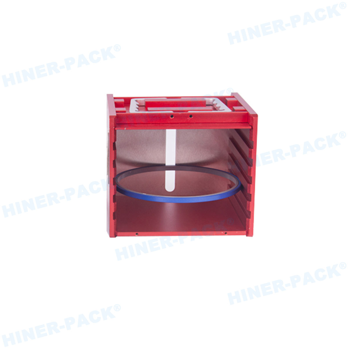
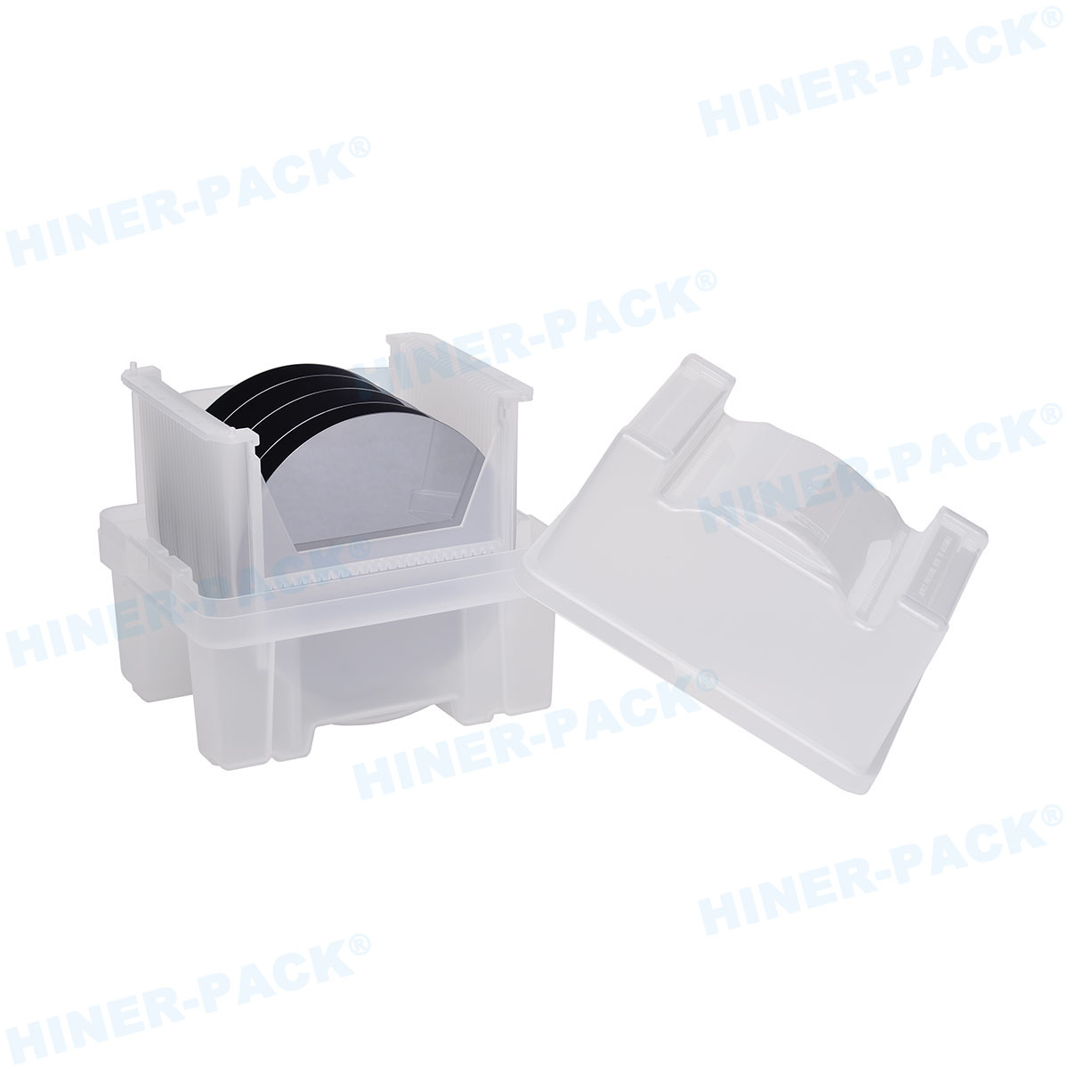
A silicon wafer container is a specialized storage and transport unit designed to hold silicon wafers securely during various stages of semiconductor fabrication. These containers, often referred to as front-opening unified pods (FOUPs) or standard mechanical interface (SMIF) pods, are engineered to protect wafers from contaminants, physical damage, and environmental factors such as humidity, static electricity, and particles. The primary purpose of a silicon wafer container is to maintain the pristine condition of wafers, which are typically thin, fragile discs of silicon used as substrates for integrated circuits. In modern fabs (fabrication plants), even a single particle of dust can ruin a wafer worth thousands of dollars, making the silicon wafer container a cornerstone of quality control. By providing a controlled microenvironment, these containers help prevent defects, reduce scrap rates, and enhance overall production efficiency. Moreover, the silicon wafer container facilitates automation in handling systems, allowing robotic arms to seamlessly load and unload wafers without human intervention, thus minimizing the risk of contamination and errors. As semiconductor technology advances toward smaller nodes (e.g., 5nm and below), the demand for highly reliable silicon wafer container solutions continues to grow, underscoring their critical role in the industry.
How Are Silicon Wafer Containers Designed for Maximum Protection?
The design of a silicon wafer container is a marvel of engineering, tailored to address the unique challenges of wafer protection and handling. Typically, these containers feature a front-opening mechanism that allows easy access while maintaining a sealed environment. The interior includes precisely spaced slots to hold wafers in place, preventing contact and minimizing stress that could lead to breakage. Key design elements include:
Material Selection: High-purity plastics, such as polycarbonate or polyetheretherketone (PEEK), are commonly used to construct silicon wafer container units. These materials are chosen for their low particle generation, chemical resistance, and ability to withstand sterilization processes.
Sealing Systems: Advanced gaskets and latches ensure an airtight seal, protecting wafers from airborne contaminants and moisture. Some silicon wafer container models incorporate purge ports for introducing inert gases like nitrogen to create a clean atmosphere.
Ergonomics and Compatibility: The design aligns with industry standards (e.g., SEMI standards) to ensure interoperability with automated equipment. This includes standardized dimensions and interface points for robotic handling.
Static Control: Built-in features to dissipate static electricity prevent electrostatic discharge (ESD), which can damage sensitive circuits on the wafers.
Through iterative testing and innovation, the silicon wafer container has evolved to support larger wafer sizes (e.g., 300mm and 450mm) and higher throughput, making it a pivotal component in scaling semiconductor production.
What Materials Are Used in Silicon Wafer Containers and How Do They Impact Performance?
The materials used in a silicon wafer container are carefully selected to meet stringent purity and durability requirements. Common materials include engineered polymers and composites that offer low outgassing, high strength, and resistance to chemicals used in cleaning processes. For instance, carbon-filled plastics may be employed to enhance conductivity and reduce ESD risks. The choice of material directly impacts the performance of the silicon wafer container in several ways:
Contamination Control: Materials with smooth surfaces and minimal shedding help maintain the cleanroom environment, which is crucial for wafer integrity. A high-quality silicon wafer container will have undergone rigorous testing to ensure it does not introduce particles or ionic contaminants.
Thermal Stability: Semiconductor processes often involve extreme temperatures; thus, the silicon wafer container must withstand thermal cycling without deforming or degrading.
Longevity and Cost-Efficiency: Durable materials extend the lifespan of the silicon wafer container, reducing replacement frequency and overall operational costs.
By leveraging advanced material science, manufacturers continuously improve the silicon wafer container to align with the evolving demands of the semiconductor industry, such as compatibility with new fabrication techniques like EUV lithography.
How Does a Silicon Wafer Container Integrate into the Semiconductor Manufacturing Workflow?
In the complex semiconductor manufacturing workflow, the silicon wafer container serves as a protective vessel that accompanies wafers through multiple stages, including lithography, etching, deposition, and inspection. Its integration is seamless, thanks to standardized interfaces that allow for automated transfer between tools. The silicon wafer container is typically loaded in a cleanroom environment and then transported via overhead hoists or automated guided vehicles (AGVs) to various processing stations. During each transfer, the container remains closed to preserve the internal environment, only opening when necessary under controlled conditions. This minimizes exposure to potential contaminants and ensures consistent yield. Additionally, the silicon wafer container often includes RFID or barcode tags for tracking and traceability, enabling real-time monitoring of wafer lots. This integration not only enhances efficiency but also supports lean manufacturing principles by reducing handling time and errors. As fabs adopt Industry 4.0 technologies, the silicon wafer container is becoming smarter, with sensors that monitor internal conditions like temperature and humidity, further optimizing the manufacturing process.
What Are the Best Practices for Cleaning and Maintaining Silicon Wafer Containers?
Proper cleaning and maintenance of a silicon wafer container are essential to prevent cross-contamination and ensure long-term reliability. Best practices involve regular inspection and cleaning cycles using validated procedures. Typically, this includes:
Automated Cleaning Systems: Many fabs use specialized washers that employ deionized water, surfactants, and ultrasonic agitation to remove particles and residues from the silicon wafer container. The process must be gentle yet effective to avoid damaging the container.
Validation and Testing: After cleaning, the silicon wafer container undergoes particle count tests and surface analysis to verify cleanliness levels meet specifications (e.g., ISO Class 1 cleanroom standards).
Storage and Handling: When not in use, the silicon wafer container should be stored in a clean, dry environment to prevent contamination buildup. Staff training on proper handling techniques is crucial to avoid mishandling that could compromise the container's integrity.
By adhering to these practices, companies can extend the life of their silicon wafer container inventory and maintain high production standards, ultimately protecting their investment in semiconductor manufacturing.
What Future Trends Are Shaping the Development of Silicon Wafer Containers?
The future of the silicon wafer container is being shaped by trends such as miniaturization, sustainability, and digitalization. As wafer sizes increase and feature sizes shrink, containers must evolve to handle higher densities and more sensitive wafers. Innovations include the development of lightweight materials to reduce shipping costs and carbon footprint, as well as smart containers with embedded IoT sensors for predictive maintenance and real-time data analytics. Furthermore, the push toward circular economy models is driving the design of recyclable and reusable silicon wafer container solutions. These advancements ensure that the silicon wafer container remains a vital enabler of semiconductor progress, adapting to the industry's dynamic needs.
In summary, the silicon wafer container is a critical component in semiconductor manufacturing, offering protection, efficiency, and integration across the production chain. By understanding its functions, design, materials, and maintenance, stakeholders can optimize their processes and stay competitive in a rapidly evolving field.
Frequently Asked Questions About Silicon Wafer Containers
Q1: What is the primary purpose of a silicon wafer container?
A1: The primary purpose of a silicon wafer container is to protect silicon wafers from contamination, physical damage, and environmental factors during storage and transport in semiconductor manufacturing. It ensures wafers remain in a controlled, clean environment to maintain high yield and quality.
Q2: How often should a silicon wafer container be cleaned?
A2: A silicon wafer container should be cleaned after each use or according to a scheduled maintenance plan, typically based on the fab's cleanliness protocols and the container's exposure to contaminants. Regular cleaning prevents particle buildup and ensures optimal performance.
Q3: Can silicon wafer containers be reused?
A3: Yes, silicon wafer containers are designed for multiple uses. With proper cleaning and maintenance, they can be reused many times, making them a cost-effective and sustainable solution in semiconductor operations.
Q4: What standards govern the design of silicon wafer containers?
A4: Silicon wafer containers adhere to industry standards set by organizations like SEMI (Semiconductor Equipment and Materials International), which specify dimensions, materials, and performance criteria to ensure compatibility and safety across different manufacturing tools.
Q5: How do silicon wafer containers contribute to automation in fabs?
A5: Silicon wafer containers feature standardized interfaces that allow seamless integration with robotic handling systems, enabling automated loading, unloading, and transport. This reduces human intervention, minimizes contamination risks, and increases throughput in semiconductor fabrication facilities.


