Silicon wafers are the foundation of the semiconductor industry, serving as the base for microchips and electronic devices. Given their extreme fragility and sensitivity to contaminants, the safe transportation of these wafers is paramount. This is where silicon wafer shipping containers come into play. These specialized containers are designed to protect wafers from physical damage, electrostatic discharge, and environmental contaminants during transit and storage. In this article, we will explore five essential aspects of silicon wafer shipping containers that highlight their importance, design, and functionality. Whether you are in manufacturing, logistics, or quality control, understanding these elements can help optimize your processes and safeguard valuable components.
Materials and Construction of Silicon Wafer Shipping Containers
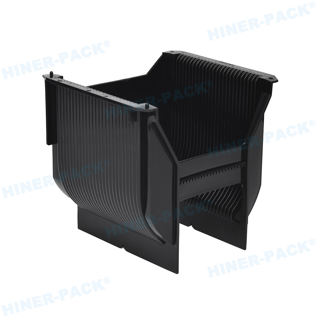
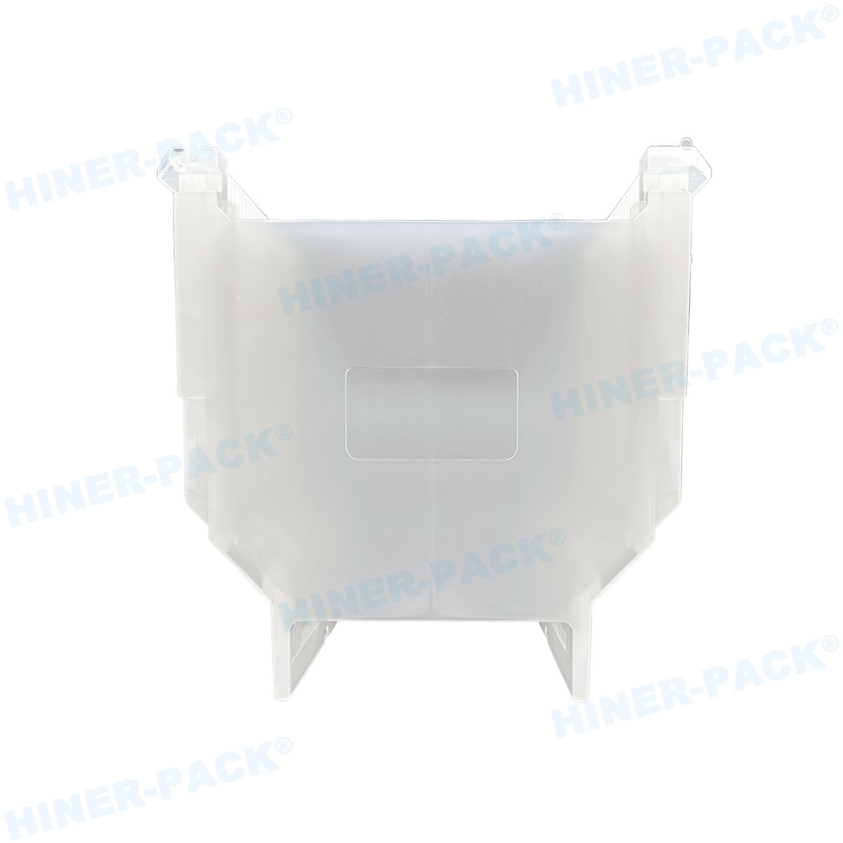
The materials used in silicon wafer shipping containers are critical to their performance and durability. Typically, these containers are made from high-grade plastics such as polycarbonate, polypropylene, or other engineered polymers that offer a combination of strength, lightweight properties, and resistance to chemicals. These materials are chosen for their ability to withstand harsh handling conditions while maintaining structural integrity. For instance, polycarbonate is known for its impact resistance, which is essential for preventing cracks or breaks in the wafers during shipping. Additionally, many silicon wafer shipping containers incorporate anti-static additives to dissipate electrostatic charges, reducing the risk of electrostatic discharge (ESD) that could damage sensitive wafers. The construction often includes precision-molded parts that ensure a snug fit for the wafers, minimizing movement and friction. Some advanced containers feature transparent lids or bodies, allowing for visual inspection without exposing the wafers to contaminants. The choice of materials also considers factors like temperature stability, as silicon wafer shipping containers may be exposed to varying environmental conditions during transit. By using robust and tailored materials, manufacturers ensure that these containers provide reliable protection, thereby extending the lifespan of the wafers and reducing waste in the supply chain.
Protection Mechanisms in Silicon Wafer Shipping Containers
One of the primary functions of silicon wafer shipping containers is to offer comprehensive protection against various hazards. This includes physical shocks, vibrations, and ESD, which are common during transportation. To address physical impacts, these containers often include cushioned interiors, such as foam inserts or spring-loaded mechanisms, that absorb shocks and prevent the wafers from shifting. For example, many silicon wafer shipping containers use custom-fit slots or cassettes that hold each wafer individually, reducing the risk of contact and scratches. ESD protection is another crucial aspect; containers are designed with conductive or dissipative materials that ground any static electricity, safeguarding the wafers from potential damage that could render them useless. Moreover, silicon wafer shipping containers may feature sealing gaskets or lids that create a barrier against moisture, dust, and other contaminants. In some cases, containers are equipped with humidity indicators or desiccant packs to control the internal environment, especially for wafers that are sensitive to moisture. The integration of locking mechanisms ensures that the containers remain securely closed during handling, preventing accidental openings. By incorporating these multi-layered protection features, silicon wafer shipping containers help maintain the integrity and performance of silicon wafers, which is essential for high-yield production in industries like electronics and solar energy.
Sizing and Compatibility for Different Wafer Sizes
Silicon wafer shipping containers are designed to accommodate a range of wafer sizes, from small diameters like 100mm to larger ones such as 300mm or even 450mm, which are common in advanced semiconductor fabrication. Standardization is key here, as the industry follows specifications set by organizations like SEMI (Semiconductor Equipment and Materials International). These standards ensure that silicon wafer shipping containers are compatible with automated handling systems in manufacturing facilities, reducing the need for manual intervention and minimizing the risk of human error. For instance, containers for 300mm wafers often include features like standardized notches and alignment pins that facilitate robotic loading and unloading. Additionally, the internal dimensions of silicon wafer shipping containers are precisely calibrated to prevent wafer bowing or warping, which can occur if the fit is too tight or loose. Some containers are modular, allowing for adjustments to handle multiple wafer sizes with interchangeable components. This flexibility is particularly valuable in research and development settings where wafer dimensions may vary. When selecting silicon wafer shipping containers, it's important to consider not only the current wafer size but also future scalability, as upgrading container systems can be costly. By ensuring proper sizing and compatibility, companies can streamline their logistics and enhance overall efficiency in wafer processing and distribution.
Cleanliness and Contamination Control
In the semiconductor industry, even microscopic contaminants can lead to defects in wafers, resulting in significant financial losses. Therefore, silicon wafer shipping containers are engineered to maintain a high level of cleanliness throughout the shipping and storage processes. This is achieved through materials that are low in outgassing and particulate shedding, as well as designs that minimize internal surfaces where contaminants could accumulate. Many silicon wafer shipping containers undergo rigorous cleaning procedures before use, such as ultrasonic cleaning or plasma treatment, to remove any residues. Additionally, containers may feature smooth, non-porous surfaces that are easy to clean and sterilize, reducing the risk of cross-contamination between batches. For critical applications, silicon wafer shipping containers are used in controlled environments like cleanrooms, where they help preserve the wafer's purity by acting as a barrier against external pollutants. Some advanced containers include integrated monitoring systems, such as particle counters or environmental sensors, to track cleanliness levels in real-time. Regular maintenance and inspection of silicon wafer shipping containers are also essential; this includes checking for wear and tear that could compromise their integrity. By prioritizing contamination control, these containers play a vital role in ensuring that silicon wafers meet the stringent quality standards required for high-performance electronic devices.
Cost-Effectiveness and ROI of Quality Containers
While high-quality silicon wafer shipping containers may involve a higher initial investment, they often prove cost-effective in the long run by reducing wafer damage, minimizing reject rates, and enhancing operational efficiency. For example, a durable container that protects wafers from ESD and physical shocks can prevent losses that might otherwise occur during transit, saving companies thousands of dollars in replacement costs and downtime. Moreover, standardized silicon wafer shipping containers can integrate seamlessly with existing automation systems, lowering labor costs and increasing throughput. The return on investment (ROI) for these containers is also influenced by their reusability; many are designed for multiple cycles, with robust construction that withstands repeated use without degradation. Companies should consider factors like container lifespan, maintenance requirements, and compatibility with logistics partners when evaluating cost-effectiveness. In some cases, custom silicon wafer shipping containers tailored to specific needs can further optimize costs by reducing waste and improving fit-for-purpose performance. Additionally, investing in quality containers can enhance a company's reputation for reliability, leading to stronger customer relationships and repeat business. By analyzing the total cost of ownership—including purchase price, maintenance, and potential savings from reduced damage—businesses can make informed decisions about silicon wafer shipping containers that align with their budgetary and operational goals.
In summary, silicon wafer shipping containers are indispensable tools in the semiconductor supply chain, offering protection, compatibility, cleanliness, and cost savings. From their carefully selected materials and advanced protection mechanisms to their standardized sizing and contamination control features, these containers address the unique challenges of transporting delicate silicon wafers. By understanding these five critical aspects, industry professionals can make better choices in selecting and maintaining silicon wafer shipping containers, ultimately safeguarding their investments and ensuring the smooth flow of production. As technology evolves, continued innovation in container design will likely further enhance their role in supporting the global electronics industry.
Frequently Asked Questions (FAQ)
Q1: What materials are commonly used in silicon wafer shipping containers?
A1: Silicon wafer shipping containers are typically made from high-performance plastics like polycarbonate or polypropylene, which offer durability, impact resistance, and anti-static properties. These materials help protect wafers from physical damage and electrostatic discharge during transport.
Q2: How do silicon wafer shipping containers prevent electrostatic discharge?
A2: They incorporate conductive or dissipative materials that safely ground static electricity, often through built-in features like carbon-loaded polymers or metal components. This design minimizes the risk of ESD, which can harm sensitive silicon wafers.
Q3: Are silicon wafer shipping containers reusable?
A3: Yes, many silicon wafer shipping containers are designed for multiple uses, with robust construction that withstands repeated handling. However, regular inspection and cleaning are recommended to maintain their protective qualities and prevent contamination.
Q4: What standards govern the sizing of silicon wafer shipping containers?
A4: The sizing is often based on industry standards set by organizations like SEMI, which specify dimensions for different wafer sizes (e.g., 200mm, 300mm). This ensures compatibility with automated systems and reduces handling errors in manufacturing environments.
Q5: How can I ensure the cleanliness of silicon wafer shipping containers?
A5: Maintain cleanliness by using containers with smooth, non-porous surfaces, performing regular cleaning (e.g., with solvents or in cleanrooms), and storing them in controlled environments. Some containers also come with desiccants or seals to minimize contamination risks.


